Essential information for understanding and designing the hardware needed for an I2C bus.
Supporting Information
Sometimes a Little Complexity Is a Good Thing
The I2C protocol is notable for some less-than-straightforward characteristics: You don’t just connect a few IC pins together and then let the low-level hardware take over as you read from or write to the appropriate buffer, as is more or less the case with SPI (Serial Peripheral Interface) or a UART (Universal Asynchronous Receiver/Transmitter). But I2C’s complexity is not without purpose; the rest of this article will help you to understand the somewhat nuanced hardware implementation details that make I2C such a versatile and reliable option for serial communication among multiple independent ICs.
The Open Drain
A defining characteristic of I2C is that every device on the bus must connect to both the clock signal (abbreviated SCL) and the data signal (abbreviated SDA) via open-drain (or open-collector) output drivers. Let’s take a look at what this actually means. First consider the typical CMOS (inverting) output stage:
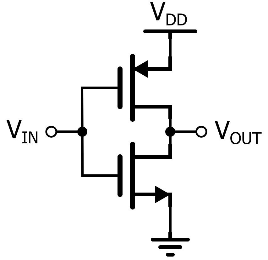
If the input is logic high, the NMOS transistor is on and the PMOS transistor is off. The output thus has a low-impedance connection to ground. If the input is logic low, the situation is reversed, and the output has a low-impedance connection to VDD. This is referred to as a push-pull output stage, though this name is not particularly informative because it does not emphasize the low-impedance nature of the connections that control the output. In general, you cannot directly connect two push-pull outputs because current will flow freely from VDD to ground if one is logic high and the other is logic low.
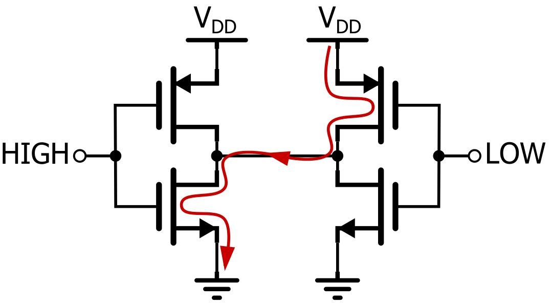
Now consider the open-drain output configuration:
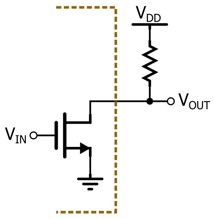
The PMOS transistor has been replaced by a resistor external to the IC. If the input is logic high, the NMOS transistor provides a low-impedance connection to ground. But if the input is logic low, the NMOS looks like an open circuit, which means that the output gets pulled up to VDD through the external resistor. This arrangement leads to two important differences. First, nontrivial power consumption occurs when the output is logic low, because current flows through the resistor, through the channel of the NMOS transistor, to ground (in the push-pull configuration, this current is blocked by the high impedance of the off-state PMOS transistor). Second, the output signal behaves differently when it is logic high because it is connected to VDD through a much higher resistance (usually at least 1 kΩ). This feature makes it possible to directly connect two (or more) open-drain drivers: even if one is logic low and the other is logic high, the pull-up resistor ensures that current does not flow freely from VDD to ground.
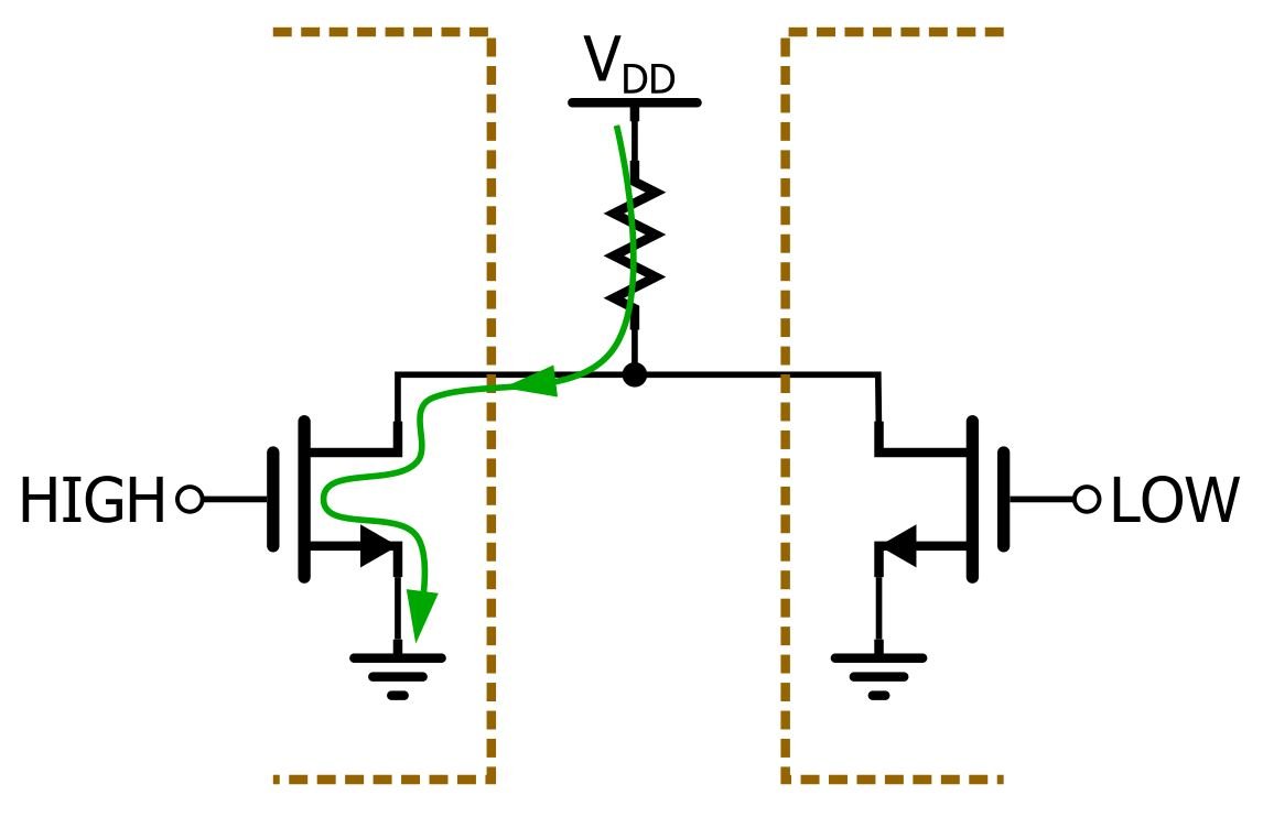
Here are three important implications of this open-drain bus configuration:
- The signals always default to logic high. For example, if an I2C master tries to communicate with a slave device that has become nonfunctional, the data signal never enters an undefined state. If the slave is not driving the signal, it will be read as logic high. Likewise, if a master device loses power during the middle of a transmission, the SCL and SDA will return to logic high. Other devices can determine that the bus is available for new transmissions by observing that both SCL and SDA have been logic high for a certain amount of time.
- Any device on the bus can safely drive the signals to logic low, even if another device is trying to drive them high. This is the basis of I2C’s “clock synchronization” or “clock stretching” feature: the master generates the serial clock, but if necessary a slave device can hold SCL low and thereby decrease the clock frequency.
- Devices with different supply voltages can coexist on the same bus, as long as the lower-voltage devices will not be damaged by the higher voltage. For example, a 3.3 V device can communicate with a 5 V device if SCL and SDA are pulled up to 5 V—the open-drain configuration causes the logic-high voltage to reach 5 V, even though the 3.3 V device cannot drive 5 V from a typical push-pull output stage.
If You Have R, You Have RC
The open-drain output driver is by no means the standard configuration among digital ICs, and with good reason: it comes with some significant disadvantages. One of these disadvantages becomes apparent when we recall that capacitance is everywhere. Voltage changes are constrained by the time required to charge or discharge the capacitance associated with a particular node. The trouble is, the pull-up resistors on SCL and SDA limit the amount of charging current—in other words, we have much more R in the RC time constant that governs the transition from logic low to logic high.
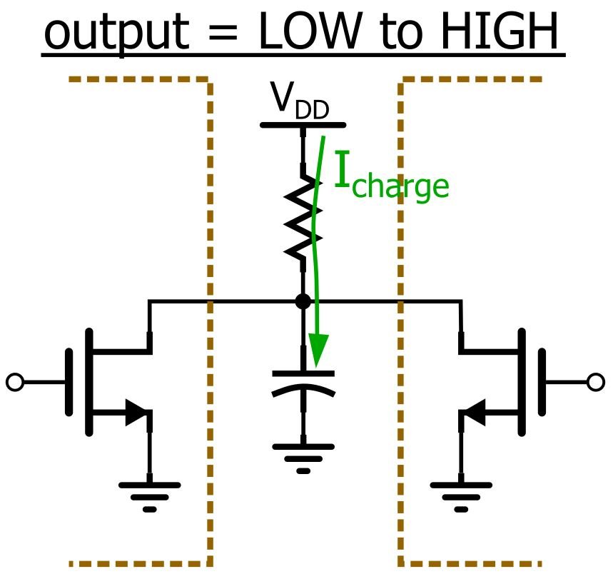
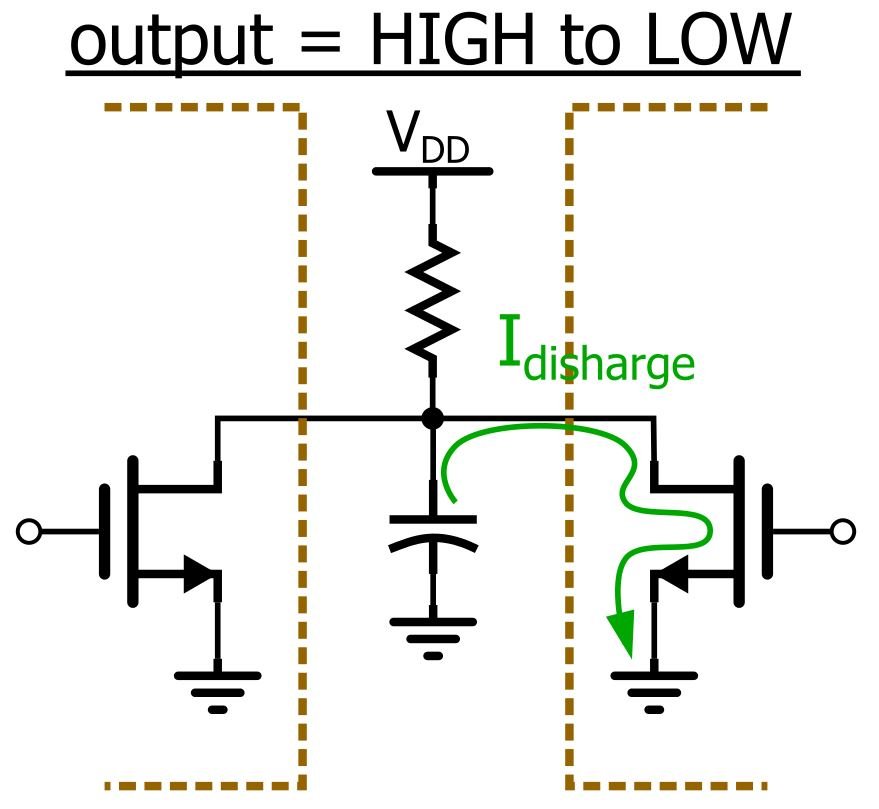
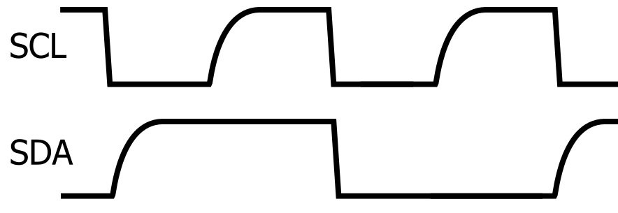
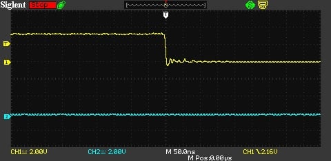
As these diagrams indicate, the low-to-high transition will be significantly slower than the high-to-low transition, resulting in the classic I2C “sawtooth” waveforms:
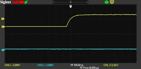
These two scope captures show the low-to-high and high-to-low transition for an I2C clock signal with a 1 kΩ pull-up resistor and minimal capacitance (only two devices on the bus, with short PCB traces).
How to Size the Pull-Up Resistors
At this point it should be apparent that the pull-up resistance imposes limitations on the maximum clock frequency of a particular I2C bus. Actually, both resistance and capacitance are factors here, though we have little control over capacitance because it is determined primarily by how many devices are on the bus and the nature of the interconnections between these devices. This leads to the enduring question, “What value of pull-up resistor should I use?” The trade-off is speed vs. power dissipation: lower resistance reduces the RC time constant but increases the amount of current that flows from VDD to ground (through the pull-up resistor) whenever SCL or SDA is logic low.
The official I2C specification (page 9) states that a voltage is not considered “logic high” until it reaches 70% of VDD. You may recall that the RC time constant tells us how long it will take a voltage to reach approximately 63% of the final voltage. Thus, for simplicity we will assume that R×C tells us how long it will take the signal to rise from a voltage near ground potential to the logic-high voltage.
Now how do we find the capacitance? The “easy” way is to assemble the entire system and measure it; at least, this is probably easier than trying to perform an accurate calculation that accounts for every source of capacitance—as an app note from Texas Instruments expresses it, “in the normal construction of electrical circuits, an unimaginable number of capacitors are formed.” If the measurement approach is not an option (as is often the case), you can make a rough estimate by finding the pin capacitance for each device on the bus (hopefully the datasheet doesn’t let you down here) and then adding 3 pF per inch of PCB trace and 30 pF per foot of coaxial cable (these numbers are from the same app note, page 3).
Let’s say we have 50 pF of bus capacitance and we want to obey the I2C “standard mode” specifications, which state that the maximum rise time is 1000 ns.
So you can satisfy the spec with Rpull-up = 20 kΩ; this value also gives you the minimum power consumption. What about speed? Let’s say you want the clock-high time to be at least triple the rise time.
If 167 kHz isn’t fast enough, you can lower the resistance (at the cost of increased power consumption) until you reach your desired clock speed. (Actually, “standard mode” limits the clock speed to 100 kHz, but you can adapt these specs to the needs of your system.)
These are rough calculations, but honestly, you don’t need to stress out about finding the perfect resistance. This general approach can help you to settle on a reasonable value, and you can always swap in different resistors if something isn’t working the way you want.
Conclusion
If this article has served its purpose, you are now thoroughly familiar with the salient details involved in I2C hardware design. We will look at firmware implementation in a separate article.
