Conventional silicon field-effect transistors (FETs) are gradually approaching their limits in terms of performance, speed, and power efficiency. At the end of 2021, a collaboration between IBM Research and Samsung Electronics led to a new class of transistors that could help to circumvent some of the scaling-related limitations associated with existing complementary metal-oxide semiconductors (CMOS).
These new transistors, dubbed vertical-transport nanosheet field-effect transistors (VTFETs), could lead to significant improvements in both performance and area scaling, potentially cutting device energy use by as much as 85% compared to the scaled FinFET architecture, according to IBM.
We spoke with Brent Anderson and Hemanth Jagannathan at IBM, two of the researchers who created VTFETs, to find out more about the new transistor and its manufacturing process.

Brent Anderson (left), Senior Technical Staff for Semiconductor Research, and Hemanth Jagannathan (right), Principal Research Staff Member.
Before we start discussing your recent work, could you tell us a little bit about your role at IBM?
Brent Anderson: I joined IBM in ‘91 and have since worked on many technologies and have held leadership roles in over ten technology nodes. I have worked with the research team here on VTFET for more than five years and prior to that, I drove technology design points, targets, and goals for other logic nodes.
I started the work on VTFET about a decade ago, then brought it into our hardware development cycle. So, when it comes to VTFET, I'm kind of the one-stop shop for the broad picture, while Hemanth is the expert on process flow and hardware results.

IBM researcher carrying a reticle mask across the track, feeding the NXE3400 EUV tool behind the track.
Hemanth Jagannathan: I joined IBM 15 years ago and worked on early materials research of high-K metal gate technology for both planar and FinFET technologies. I managed process technology groups that were responsible to introduce new materials for various logic technologies at IBM Research.
Since the early days of hardware research, I have been the hardware technologist and development manager for the VTFET program. In my role, I have worked hand in hand with IBM and Samsung colleagues. I have driven the VTFET team to bring novel ideas in this project from paper into practice with functional silicon hardware demonstration.
Recently, you were involved in a project that led to the first vertical-transport nanosheet field-effect transistors (VTFETs). What inspired your team to create these devices?
Anderson: A decade ago, we already knew that we were going to hit scaling challenges with lateral FETs and we could see the barriers as we tried to shrink the technology from node to node. In lateral FETs, you have a gate and spacers, plus contacts. There are physical limits as you scale them, which effectively limits scaling beyond 40nm.
The motivation for VTFETs was to find a solution to continue Moore's law scaling beyond this 40nm contacted gate pitch (CGP), the minimum distance from one transistor's gate to another transistor's gate. When we move to a vertical orientation, we can make the gates longer and the source-drains and spacers thicker, and this reduces the resistance and capacitance. So not only do we get smaller, but we are also able to obtain higher performance.
What are the primary advantages of the new semiconductor architecture? What are its characterizing features?
Anderson: FinFETs replaced planar because they had a much better gate control and the CGP could shrink from about 90nm to 48nm. As we continue to scale the CGP, however, we run into a number of issues, particularly with gate control. That's where nanosheets come in—with 50nm to 40nm CGPs.
With nanosheets, we get rid of the quantization, achieve tighter control over the thickness of the Fin, and move to a gate that surrounds the channel, which means we can shrink the CGP further. Yet, at an approximately 40nm gate pitch, we run out of room. The gate length, for example, becomes too difficult to control.
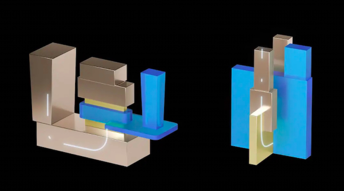
With VTFET, the gate completely wraps around the Fin and now that the Fin (sheet) is vertical, we can now make the gate as long as we want. The spacers that isolate the gate from the source and drain are thicker and the source-drains are also thicker, lowering resistances.

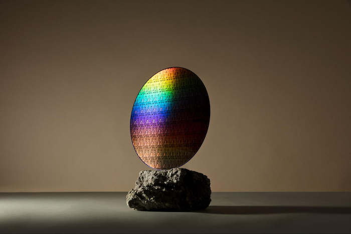
VTFET wafer.
Other unique features of VTFETs are the contacts to the bottom source-drain, the top source-drain, and the gate. Because there is more room, we can make the contacts larger, lowering resistance values and moving them farther apart, attaining lower capacitance and very good yield. And, because the features are now vertical, there is now more space separating the features, allowing us to scale the technology going forward.
To isolate circuits in lateral FETs, we need to insert a dummy isolation gate, a special gate that electrically isolates one circuit from the next and wastes a lot of space. With VTFET, we instead introduced small oxide trenches that isolate adjacent circuits. This means more scaling possibilities because we do not require extra dummy gates to isolate individual circuits.

Timeline summarizing crucial technologies introduced by IBM over the years.
Jagannathan: The CGP is the metric we use to compare different architectures. We demonstrated CGPs for VTFETs that are far more aggressive than what is currently in production, which is quite uncharacteristic for a first hardware research paper. Flipping the orientation of current flow (versus the substrate) creates more space for contacts and freedom to define gate length. It also optimizes device capacitance and allows for unique isolation of adjacent transistors without having dummy gates. We call this unique isolation technique zero-diffusion break (ZDB).
How does this architecture compare to conventional FinFET technologies?
Jagannathan: When developing new transistors architectures, you want higher density, so you can fit more transistors within a given area and attain higher performance and energy efficiency. When a lateral FET architecture, such as FinFET, is forced to fit within a 40nm CGP, there will be obvious degradation in the device’s characteristics. You will be forced to have thin spacers, very short gate lengths, and limited space for the contacts. All of these challenges will have a direct impact in terms of performance and power.
With VTFET, we are able to get a higher density because of the zero-diffusion break (ZDB). We can bring circuits closer together, remove the dummy gates, and reduce the gate pitch. Because the contacts are now large, we can tune the size of the contacts independently and reduce the resistance of the top and bottom contacts by almost half.

Comparison of a VTFET (left) vs. a lateral FET (right) transistor with current flowing through them.
The structure itself has independent knobs to tune the various parameters, so we are also able to achieve a 50% reduction in capacitance. That in itself is huge because it translates to two times higher performance compared to a FinFET device in the same regime. And in scenarios where you want to trade off performance with energy, you can have an equivalent performance with an 85% power reduction. So it's either-or, but you can go somewhere in between if the product requires that.
Moreover, by flipping the gate and channel vertically, we are also able to optimize the spacer size so you can have larger spacers, which means you can tolerate higher voltages, broadening the device’s operational regime.
What were some of the main challenges you encountered while developing the transistors? How were you able to overcome them?
Anderson: Moving to a vertical orientation changes the development process quite a bit. For example, vertical spacers need to be defined very differently than lateral spacers. The top source-drain plus spacers are also very new and different.
One of the fundamental characteristics that we chose to address early is self-alignment. For the zero-diffusion break, we introduced very narrow trenches using a new self-alignment technique instead of patterning. This entailed different integration requirements, even if the necessary tools are actually similar to what we use today.

VTFET wafer closeup.
Jagannathan: VTFET is a revolutionary device because the way we build it is unlike any other method used in the past. While this offers the benefit of special features, it also poses the challenge of how to integrate them. Each module has a unique fingerprint and building it required unique considerations.
The bottom and top source-drain are formed by epitaxy and at different points in time. All logic transistors to date have formed the source and drain at the same time (i.e., they are symmetric in nature). In our case, the junctions are asymmetric in nature since the modules following the bottom source-drain formation can start impacting the junction and make it quite different from the top junction formed later in the process flow. The device presented in our paper is the result of many years of iterations and optimizations.
When will we see the new transistors come to market?
Anderson: FinFET is the most advanced technology on the market today. Nanosheet is expected to come out in just a few years and last for several nodes. The timing for VTFET is after nanosheet, so many years will pass before it makes it into the market. We presented the paper to prepare the industry so when it launches, the infrastructure will be available and it will be a successful technology.
Cell phones are one of the largest markets that are most likely to introduce this type of product.
The transistors were the result of a collaboration between IBM and Samsung. What did the two companies contribute to the project in terms of resources and expertise?
Jagannathan: We have a very closely-knit ecosystem with our partners, such as Samsung, and our suppliers. For this project, IBM and Samsung engineers were co-located in Albany, New York, working side by side on a daily basis. Samsung is a high-volume manufacturer of semiconductor technology and while IBM currently no longer manufactures its own chips, we have deep expertise in research and innovation.

A researcher at a Thermal Compression Bonding (TCB) tool in Nano Fab South at Albany, NY.
Do you believe VTFETs are a key to extending Moore’s law?
Jagannathan: The VTFET technology that we have demonstrated shows the potential for higher performance, lower energy consumption, and higher density. We believe that VTFETs are a strong candidate post-nanosheets and provide a bright future for Moore’s law scaling for years to come—along with the recent innovations in monolithic 3D and chip stacking technology.
What are the next steps for the real-world implementation of these transistors?
Anderson: The first step was to share it with the industry to get that feedback and acceptance. We now need to continue developing the technology and make it more mature. We also shared early results for additional features besides the logic transistor where further optimization is important.
In the future, we also plan to publish design papers covering SRAMs, logic circuits, and so forth. There are still a number of steps before we're going to be ready for production, and this will fill up the next several years as we continue to move the technology forward. When we presented it at the IEEE International Electron Devices Meeting (IEDM), the feedback was excellent.
Jagannathan: Work within and outside IBM will be crucial for VTFETs' real-world adoption and implementation. As we start educating more about VTFETs, we are eager to see how the industry responds, along with the design community, suppliers, and the equipment community. All of this will hopefully start a good conversation to mature our perspectives further.
Hemanth Jagannathan, Brent Anderson, and their colleagues at IBM are continuing to explore the potential of VTFETs and are working on improving their performance. To find out more about their work visit the IBM Research website.
All images used courtesy of IBM.
