Wide bandgap oxide semiconductors are increasingly popular in optoelectronic devices, flat panel displays, solar cells, OLEDs (organic light-emitting diodes), and flexible and transparent electronics. This is because this unique class of semiconducting materials exhibits excellent electrical conductivity and optical transparency.
Now, a team of researchers from Purdue University's Elmore Family School of Electrical and Computer Engineering has found a way to develop smaller and higher-performing transistors using indium oxide semiconductors and a technique known as atomic layer deposition.

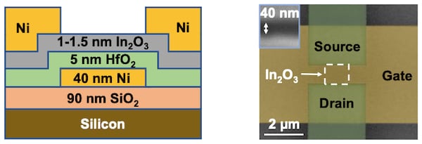
Structure of the In2O3 transistor (left) and the fabricated In2O3 transistor. Image used courtesy of Purdue University
How might this research extend Moore's law in scaling future transistor technology?
Transparent Conducting Oxides on the Rise
To explore this question, it may be useful to discuss why indium oxide was a key factor in the success of Purdue researchers.
Oxide semiconductors such as indium oxide (In2O3), zinc oxide, and cadmium oxide have a large bandgap—and are transparent in the visible range as a result. Hence, these materials are also known as transparent conducting oxides (TCOs).
Today, most transistors are silicon-based, and the atomic size of silicon material is about 0.2 nanometers. If we shrink transistors below a few nanometers in width, the conductivity of the thin film would be negligible and would not be able to handle high current density. TCOs, on the other hand, can be heavily doped to achieve high conductivity. Their optical properties are also tunable by adjusting carrier concentration. Moreover, they can be grown into thin films and many other crystalline structures.
Recently, there has been increasing research attention on indium oxide semiconductors because they can be applied in the back-end-of-line (BEOL) compatible transistors for three-dimensional integration. BEOL is the second part of the wafer, which includes contacts, dielectrics, metals, bonding sites to interconnect devices like transistors, capacitors, and resistors.
Atomic Layer Deposition
Although In2O3 has higher electron mobility than other oxide semiconductors, In2O3 films deposited by physical vapor deposition (PVD) methods can result in unstable electrical properties. Due to their high electron density, it is difficult to suppress the drain current or off-current at zero gate bias.
These limitations in creating In2O3 films are overcome by an atomic layer deposition (ALD) technique.

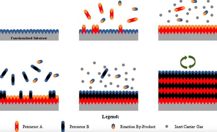
Illustration of the ALD process. Image used courtesy of ScienceDirect
ALD can deposit atomically thin-film materials onto a substrate. The technique involves exposing the surface of a substrate to alternating precursors, the compounds that produce another compound in a chemical reaction. In each alternate cycle of ALD, the precursor reacts with the surface. It then ensures that the reaction stops when all reactive sites on the surface are used.
The ALD method can be repeated multiple times to get the desired thickness of the thin film. Typically, ALD is carried out at lower temperatures since the substrates are fragile and high temperatures usually result in poor growth rates.
Purdue Researchers Advance Semiconductor Design by Shrinking Transistors
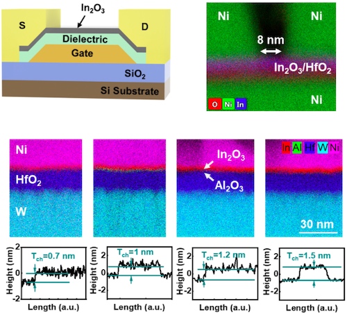
In a recent study published in Nature Electronics, the researchers from Purdue reported high-performance indium oxide transistors with channel lengths down to 40nm and with a high drain current of 2.0 A/mm at a low drain-source voltage of 0.7 V. Thanks to ALD, the channel thickness is scaled down to 1nm and has an equivalent oxide thickness (EOT) of 2.1nm. The transistors exhibit immunity to short channel effects due to the low channel thickness.
The gate of the developed transistor includes:
- Gate metal: 40nm nickel
- Gate dielectric: 5nm hafnium oxide
- Semiconducting channel: 1/1.2/1.5nm indium oxide
- Source and drain contacts: 80nm nickel

Scaled In2O3 transistor by high-resolution transmission electron microscopy and atomic force microscopy. Image used courtesy of Purdue University
According to the researchers, indium oxide-based devices are promising BEOL-compatible devices because of their high current density and excellent immunity to short-channel effects. They further report that the device performance still has room to boost any further scaling and process optimization.
