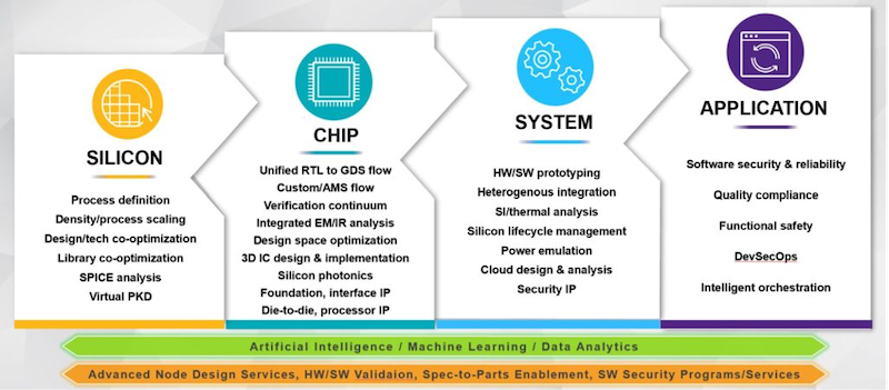
Designing and developing semiconductors that make tech innovation possible has been historically challenging. The constant evolution of electronic design automation (EDA) tools and fabrication technologies is driven by an equally growing and ever-changing set of chip complexity and sophistication demands. Some of these demands can be seen in Figure 1.

Figure 1. Examples of semiconductor design requirements. Image used courtesy of Synopsys
Adding fuel to the fire, new offerings such as mobility-as-a-service (MaaS) and autonomous vehicles rely intrinsically on data connectivity. This growing need for interconnectivity across devices and services means chips are being used in increasingly complex applications with a growing risk of security breaches, thus driving another industry tipping point.
The continuous increase in chip and system complexity, combined with higher expectations for performance and longevity, has highlighted important limitations in traditional semiconductor design and manufacturing processes.
With this concept in mind, this article will explore one potential solution of shifting from product lifecycle management (PLM) to a more specific process called silicon lifecycle management.
Shifting from PLM to SLM
For decades, companies across industries have effectively relied on PLM tools for decades to manage products from inception to market deployment. Yet, a similar process designed for silicon chips—often so closely embedded in virtually every aspect of our everyday lives from automating factories to powering our smartphones and laptops—is only now just starting to emerge.
The concept of SLM, or end-to-end silicon product management, has been gaining ground for the past few years in response to this industry gap.
Basics of Silicon Lifecycle Management
Based on the tried-and-tested PLM building blocks, SLM is an emerging concept within the industry aimed at making product development and deployment more deterministic through a cross-lifecycle approach.
SLM is also a broad process that includes monitoring and analyzing semiconductor devices as they are designed, produced, tested, and delivered into end-user systems (Figure 2).

Figure 2. An example of Synopsys’ SLM platform. Image used courtesy of Synopsys
The insights gathered from this analysis are used to optimize both the semiconductor and end-user systems throughout their product value chain, from design and manufacturing to testing and maintenance.
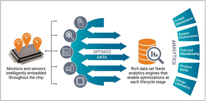
While a comprehensive platform of several tools and technologies can reap more benefits, an SLM process (Figure 3) consists of two primary phases:
- Embedding sensors, monitors, and structures in silicon designs to gain insight into device production and in-field performance
- Collecting and processing data throughout the lifecycle of silicon devices to provide analytics that can power in-design, in-production, and in-field optimizations

Figure 3. Image used courtesy of Synopsys
With SLM, semiconductor designers can deploy the “see, control, and optimize” philosophy. The embedded monitors and sensors collect and feed parametric and real-time data to engineering teams that directly translate to the improvement of a silicon system’s quality, performance, and reliability.
SLM’s ability to predict maintenance and failure in the field makes it a prime use case for hyperscaler, consumer, and automotive applications.
Current EDA Industry Challenges
The rise of SLM comes at a crucial time in the industry. Today’s accelerated scaling of device and system complexity poses a unique set of challenges to semiconductor designers.
The first challenge is how each new technology node leads to increased transistor densities, which in turn creates increased variability throughout the manufacturing process. This results in a domino effect for chip designers.
Greater manufacturing variability means chip developers need to broaden their worst-case design scope or rely on sensors and monitoring structures to measure the degrees of silicon variance.
Additionally, increased design density also produces greater current and power densities, leading to reduced and more variable node voltage supply levels and the creation of hotspots.
Today, chips and systems are becoming more intricate with different arrangements for additional routing and tracking capabilities. As more hardware and software are incorporated and continuously upgraded during in-field operation, the system-on-chip (SoC) designs’ reaction to environmental stimulus and ability to respond to varying workloads needs to be carefully managed. In turn, this generates larger volumes of data that require increased data coherency across each production stage.
As a consequence, these challenges to traditional silicon designs increase their likelihood of failure and drive the need for circuit testing beyond the manufacturing and production assessments.
The New Paradigm for SoC Systems
To respond to today’s increasing system complexity and performance demands, chip developers need to re-examine each step of their silicon device creation to amplify visibility and observability throughout its lifespan.
Embedding new, imaginative sensors and structures into the design will provide teams with more accurate data on how we screen devices for deployment during production testing and how a device will respond to dynamic environmental conditions and stimuli. Evolving data analysis throughout test phases and into operational phases could provide better insight into device failure, allowing us to perform root cause diagnosis of issues with traceable information that spans across all lifecycle phases.
SLM continues to emerge as the industry’s newest paradigm as it addresses these necessary changes in traditional silicon designs while providing insightful analysis. As the domain gathers momentum, SLM platforms will need to remain flexible, scalable, and support the easy adoption of new sensors, monitors, and data sources over time.
Key Benefits of SLM Platforms
By adopting a full-fledged SLM platform, chip developers can achieve in-depth lifecycle visibility, enriched analytics, and increased control mechanisms over their silicon devices, including dynamic voltage and frequency scaling (DVFS). The combination of these characteristics greatly optimizes device operation for power or data throughput performance (Figure 4).

Figure 4. Image used courtesy of Synopsys
However, it’s important to note that end-to-end lifecycle management is not attainable by deploying a single product or tool. The integration of varying SLM components is needed to address and provide application-specific requirements and benefits.
For instance, high-volume consumer applications can implement SLM tools and flows to reduce design constraint pessimism through parametric feedback from silicon. This allows for design tuning and gives visibility into statistical outliers and potential future failing devices.
In the context of real-time system management, highly granular thermal sensing solutions can optimize power performance in hyperscaling applications if deployed within processor cores throughout the die. This is particularly valuable for hyperscaling applications as even the slightest reduction in power consumption can result in exponential savings in large cloud server configurations. To put this into perspective, a modest improvement to thermal sensing accuracy can reduce power consumption by less than one penny per processor chip per hour. While subtle at the chip level, this minor enhancement can translate to millions of dollars in savings annually for a large data center configuration. Considering that the cost of running servers throughout their lifespan exceeds their initial purchasing price, any reduction in power consumption is impactful.
In automotive applications, the continuous assessment of aging and degradation factors, such as user mission profiles, thermal stress, and supply voltage stress will lead to a more predictive approach to the maintenance and replacement of in-vehicle electronic systems. If these systems become more deterministic for failure, commercial-grade chips can then be considered to be adopted within designs. While seemingly counterintuitive, this presents lower-cost solutions with greater determinism as opposed to more costly, hyper-reliable systems.
SLM—A New Way for Design Management
SLM represents a shift in opportunity for the semiconductor design community and the end-users in some of the most competitive markets, including automotive, data center, and consumer. Traditional semiconductor design, manufacturing, and deployment processes are being challenged on many fronts, ranging from device aging effects to regularly changing performance expectations.
A flexible concept, use cases for SLM are wide and varied. In autonomous vehicles, for example, SLM when integrated into chips can flag aging effects that degrade the silicon operating a vehicle’s braking systems, preventing potential brake failures down the line. Similarly, this approach can be applied to medical devices, where SLM can detect aging effects that impact the battery life of portable IoT devices.
System and SoC architects must embrace SLM concepts at the design, development, manufacturing, and production test stages to address today's challenges and remain competitive. While still in its infancy within the industry, the end-to-end lifecycle management approach will allow companies to utilize the most advanced silicon technologies as they emerge and maintain a path for greater semiconductor design efficiency and predictability.
Industry Articles are a form of content that allows industry partners to share useful news, messages, and technology with All About Circuits readers in a way editorial content is not well suited to. All Industry Articles are subject to strict editorial guidelines with the intention of offering readers useful news, technical expertise, or stories. The viewpoints and opinions expressed in Industry Articles are those of the partner and not necessarily those of All About Circuits or its writers.
