Chip manufacturers often try to make it incredibly simple for designers and hobbyists to implement most SMPS using modern web applications or even power design software. Backing up the software are application notes suggesting the correct PCB layout for their specific ICs.
Although the design software today is typically excellent, the problem is that most app notes can be wrong, at least partially so. In fact, several industry experts note they should be assumed wrong until proven right (1).
Furthering this idea, a keynote speech by Dr. Todd Hubing at AltiumLive 2022 covered, in part, awful converter layouts (video) and how they can cause electromagnetic compliance (EMC) failures in both conducted and radiated emissions.
To put this concept into perspective, we can go over my most recent hobbyist design, which had these hidden problems. Does it work? Absolutely. Would it pass EMC radiated and conducted emissions? Maybe.
First, let’s talk about where the problem lies, and then discuss what I did poorly in my design and how I could correct it.
A Hidden PCB Layout Threat—PCB Coupling
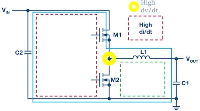
EMC principles relating to SMPS usually require that a designer pay close attention to two coupling factors, shown in Figure 1, in the layout of SMPS:
- The voltage switching node, which has a high dv/dt
- The “hot current loop,” which contains the highest di/dt in the subsystem

Figure 1. A schematic showing buck converter di/dt & dv/dt locations. Image (modified) used courtesy of Analog Devices
The mechanisms and risks at play here are capacitive (dv/dt) and inductive (di/dt) coupling of unwanted energy to other parts of the system, or worse, out of the system in the form of radiated and conducted emissions.
A PCB Design Post-production Review
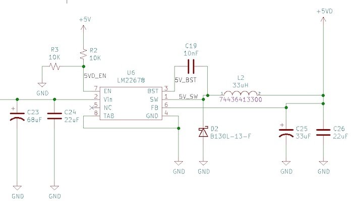
Diving into the project, we are going to examine the PCB layout of an LM22678 5A converter (Figure 2) with a Vin of 12 V (not shown) and a Vout of 5 V. This is a non-synchronous buck converter using a B130L-13-F Schottky diode for its low-side switching element (and yes, before you check—the system draws less than the 1 A rating of the diode!).

Figure 2. The schematic for a non-synchronous LM22678 buck converter 12 V to 5 V.
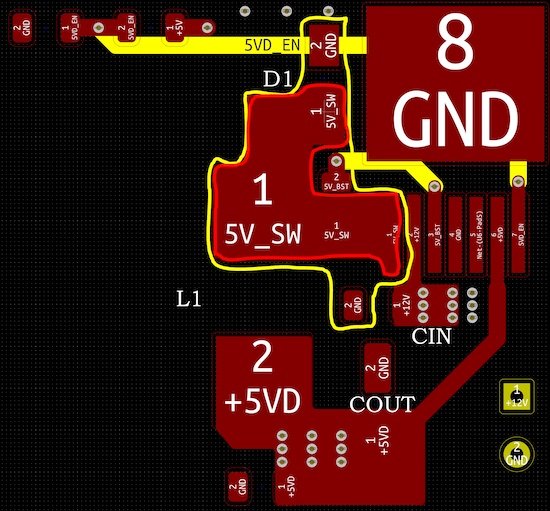
Minimizing capacitive and inductive coupling is typically not complicated but it is easy to overlook, leading to failing emissions testing and market delays. Below, in Figure 3, we see the layout of a TO-263 package for the non-synchronous buck regulator with the voltage node (red outline) and hot current loop (yellow outline) identified.

Figure 3. Non-synchronous buck regulator design with low-side power diode.
For clarity, the copper fills on the board have been hidden. Overall, there are three glaring issues with this design:
- The high di/dt loop is far larger than it needed to be
- No vias connect the GND nodes of CIN or COUT (they were ground pour covered)
- The switching node could be smaller
The net effect of these design choices means that the current loops are not well contained, and the current does not have a well-defined path back to the source due to a lack of vias between the planes.
For EMC—(Electrical) Silence Is Golden
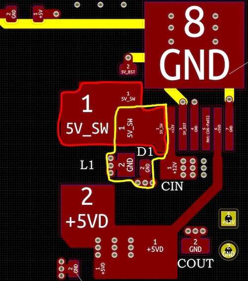
Applying the principles gleaned from Dr. Hubing’s discussion, the improved layout can be seen below in Figure 4. It features an optimized voltage node, a smaller hot loop and via access to the layer 2 reference plane for each passive component. Additionally, the primary COUT capacitor was also rotated 90 degrees relative to the original design reducing the risk of noise on the output rail.

Figure 4. The improved layout takes the coupling mechanisms into account.
By moving the low-side diode inline between the switch pin and the inductor, we are better constraining the potential crosstalk noise generated by the high dv/dt coupling effects. Further, by reducing the hot loop geometry the effects of high di/dt magnetic field coupling are decreased.
Though these changes are small, they require no additional board space or shuffling of other subsystems. However, the system compliance was undoubtedly enhanced by reducing the current loop by approximately 50% and optimizing the voltage node.
When you are designing commercial products to comply with CISPR EMC standards, every dBμV counts, and small changes at the design stage might mean the difference between a profitable launch or a missed market window.
Key Takeaways
- Understand where the current loops flow in your switched-mode power supply
- Keep node and loop geometry small to mitigate unwanted coupling effects
- Keep CIN away from or COUT to help isolate current loop induced fields, and prevent dv/dt crosstalk
- Tie pads to vias, not just ground fill copper to assist in constraining the return current
(1) The aphorism is first attributed to Lee Ritchey (1993).
