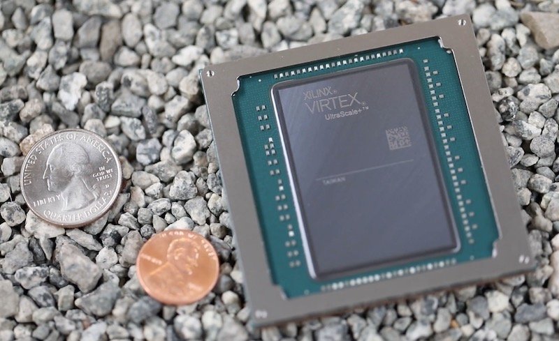
Composed of 35 billion transistors, the VU19P is the newest member of the 16 nm Virtex UltraScale+ family.
Xilinx has expanded its 16-nanometer (nm) Virtex UltraScale+ family to include the Virtex UltraScale+ VU19P. With 35 billion transistors, the VU19P is said to provide the highest logic density on any single chip that’s ever been built.
The VU19P features 9 million system logic cells, DDR4 memory bandwidth of up to 1.5 terabits per-second, transceiver bandwidth of up to 4.5 terabits per-second and more than 2,000 user I/Os.
This massive I/O bandwidth is well suited for multi-FPGA interconnection. It also enables engineers to connect a wide range of external memory types and rates to implement fast, deep storage of state information.

The VU19P. Image from Xilinx
The new device will enable designers to emulate and prototype the most advanced ASICs and SoCs. It will also streamline test and measurement, as well as cutting edge applications in defense, aerospace, and networking.
Hardware and software co-validation endows for developers with the ability to bring up software and implement custom features before physical parts are available. With the VU19P FPGA, engineers will have a tremendous advantage in the development of algorithms for artificial intelligence, machine learning and for video processing.
Today’s Challenges
The design of ASICs for AI, 5G, and autonomous driving applications requires moving massive amounts of data in order to be able to feed their complex algorithms. To meet this challenge, The VU19P includes 80 transceivers, the most ever in an emulation class device. This high transceiver count enables communication test equipment can support higher port densities.
Emulation and prototyping customers have insatiable demands for higher I/O count and memory bandwidth. The VU19P, with its more than 2,000 user I/Os, means more external memory for debug and more interconnect for environments featuring multiple FPGAs.
Faster Software Development
"The VU19P enables developers to accelerate hardware validation and begin software integration before their ASIC or SoC is available," said Sumit Shah, Senior Director of Product Line Marketing and Management at Xilinx.
This claim is backed up by Tran Nguyen, Director of Design Services at ARM. According to Nguyen, "Arm relies on Xilinx devices as part of our process for validating our next-generation processor IP and SoC technology." He goes on to state that, "The new VU19P will further enable Arm, and many others in our ecosystem, to accelerate the design, development, and validation of our most ambitious roadmap technologies."
Development Tools
Xilinx provides VU19P customers with a wide range of debug, visibility tools, and IP, providing users with a comprehensive development platform, enabling them to quickly design and validate their most complex applications and technologies.
Designers will also enjoy the benefits of Xilinx’s Vivado Design Suite in the enhancement of overall flow for design implementation. This SoC-strength development environment is touted by Xilinx as enabling designers to reduce tape-out risk, the final step in the design process preceding actual physical manufacturing.
Around the Industry
The challenges posed by AI and 5G have spawned even more interest than ever in high-performance FPGAs. Many manufacturers have entered the competition.
We recently discussed Intel’s Agilex family of FPGAs focused on data center applications. The latest version in production is the Agilex I-series. These devices are built on 10-nanometer technology. They are intended for bandwidth-intensive applications, supporting data rates of up to 112 Gbps. Coming soon from Intel will be the improved Agilex M-series FPGA.
What do you use FPGAs for in your work? Tell us about your applications in the comments below.
