Learn about the Sulzer network, an alternative to classic R-C networks that is easier to tune over wide frequency ranges.
In my previous article, I explained the classical oscillator networks you're probably familiar with: the Wien and Bridged-T networks. At the end, I explained that they are undesirable in some applications because tuning them is difficult over a wide frequency range.
In this article, I'll lay out an alternative network you may not have heard of: the Sulzer network.
Who Is Peter Sulzer?
It may surprise you to learn that back in 1952 Peter Sulzer of the National Bureau of Standards (now NIST) published in Electronics magazine an oscillator built around an innovative R-C network that can be tuned over a wide frequency range conveniently with a single variable resistor, and with a constant attenuation over frequency. This circuit can be a viable alternative to the Bridged-T oscillator, which Sulzer in fact developed a little more than a year before inventing the network that is the subject of this article.
Outside of two hobby construction articles that appeared in Popular Electronics in 1956 and The Radio Constructor in 1958, I’ve never seen this network in any textbook, despite the network being a clever circuit that eliminates the tracking problem between dual variable elements.
The Sulzer Network Topology
First, let’s look at the network topology Sulzer published—more elaborate than the traditional R-C network—with its single tuning resistor. Later, we'll compare its simulation results with that of the classical networks.
An example network with some typical component values is shown in Figure 1.
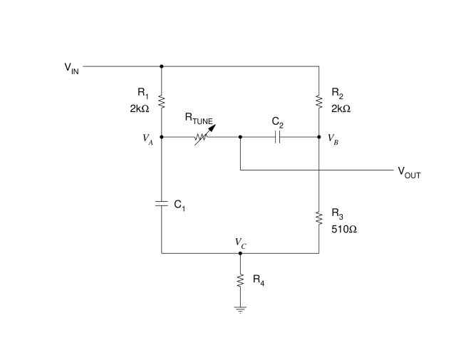
Figure 1. Sulzer’s phase shift network for R-C oscillators
As with the classical oscillators, the feedback loop output is connected to VIN of this network, and VOUT is fed back to the feedback gain block input. We’ll assume the gain block input draws negligible current from the VOUT node.
The current into the VIN terminal splits into two paths of two voltage dividers:
- A divider between R1 and C1
- A divider between R2 and R3
The two current paths join again with the total current dropped across R4 to ground.
The output voltage is formed at the common connection of the variable tuning resistor RTUNE and capacitor C2. The values of C1 and C2 determine the frequency band that the oscillator can be tuned over.
What Sulzer Modified: The All-Pass Network
Now, let’s trace through Sulzer’s original conceptual development of his network to see how the phase shift from VIN to VOUT will pass through zero at some resonant frequency.
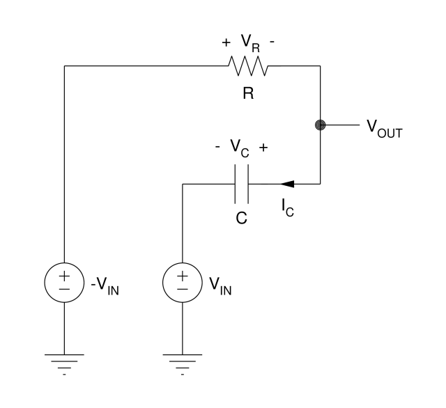
Start with the simple ideal phase shift network of Figure 2.
Figure 2. Ideal circuit for an all-pass network
This network is fed by two sinusoidal input voltage sources 180 degrees apart in phase, VIN and -VIN. The output voltage is taken from the common connection of a resistor and capacitor as shown.
This is a well-known “all-pass” network, with an output magnitude constant with frequency and equal to the input magnitude, and with the output phase varying continuously from 180 down to 0 degrees as the frequency is raised.
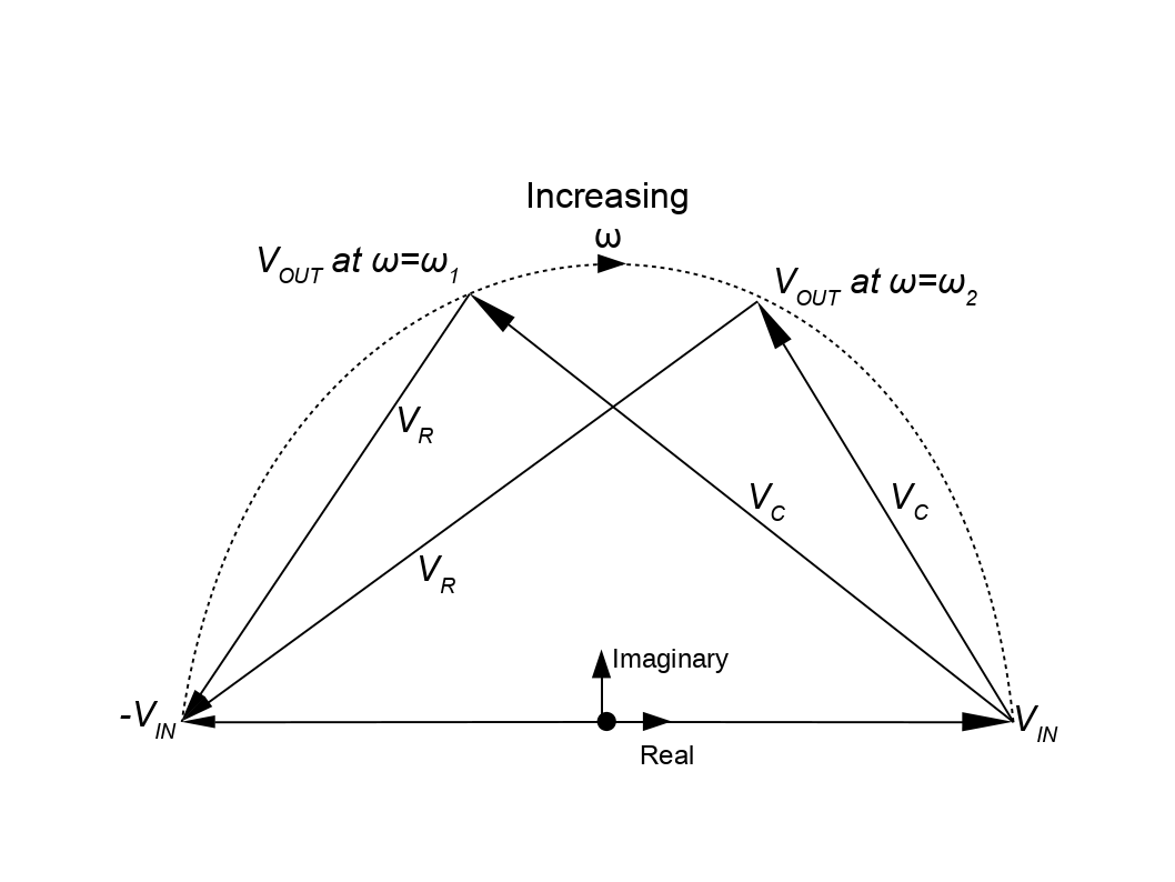
The phasor vector diagram in Figure 3 shows graphically how this all-pass network works.
Figure 3. Phasor vector diagram for the ideal all-pass network
The two phasors for the two input sources extend to the right and left on the real axis with a magnitude of VIN. Since the capacitor voltage VC and the resistor voltage VR must sum up to the total voltage between the two input sources in the circuit network, the vector sum of the phasors representing VC and VR must graphically span between the two input vectors. Two phasors representing the output voltage VOUT at the intermediate point between VC and VR are shown at two different frequencies in the figure above.
We know the vector relationship between VC and VR. Since then . Due to the factor of j in this relation, the phasors of VC and VR must graphically be at right angles, representing a 90 degree phase shift. As the frequency increases, the length of VR will increase and that of VC will decrease. The only way to satisfy these geometric constraints is for the phasor of VOUT to trace out a semicircle as shown as the frequency is increased. This implies a constant output magnitude equal to the input magnitude and a phase varying from 180 to 0 degrees.
Note that this phasor diagram does not have a path for the output phase to pass in and out of zero degrees, as do the classical networks, so a single all-pass network of this type will not be useful in an oscillator. Sulzer modified this network in search of a useful circuit that can be tuned with a single variable resistor.
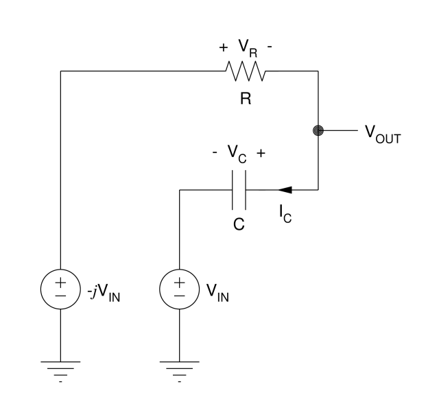
We trace his design process by replacing the -VIN source in Figure 2, a duplicate of the input voltage phase shifted by 180 degrees, with a source that is the input voltage instead shifted in phase by -90 degrees.
Mathematically, this is represented by the phasor -jVIN., as shown in the schematic of Figure 4 and the phasor diagram of Figure 5.
Figure 4. Ideal circuit for the modified all-pass network
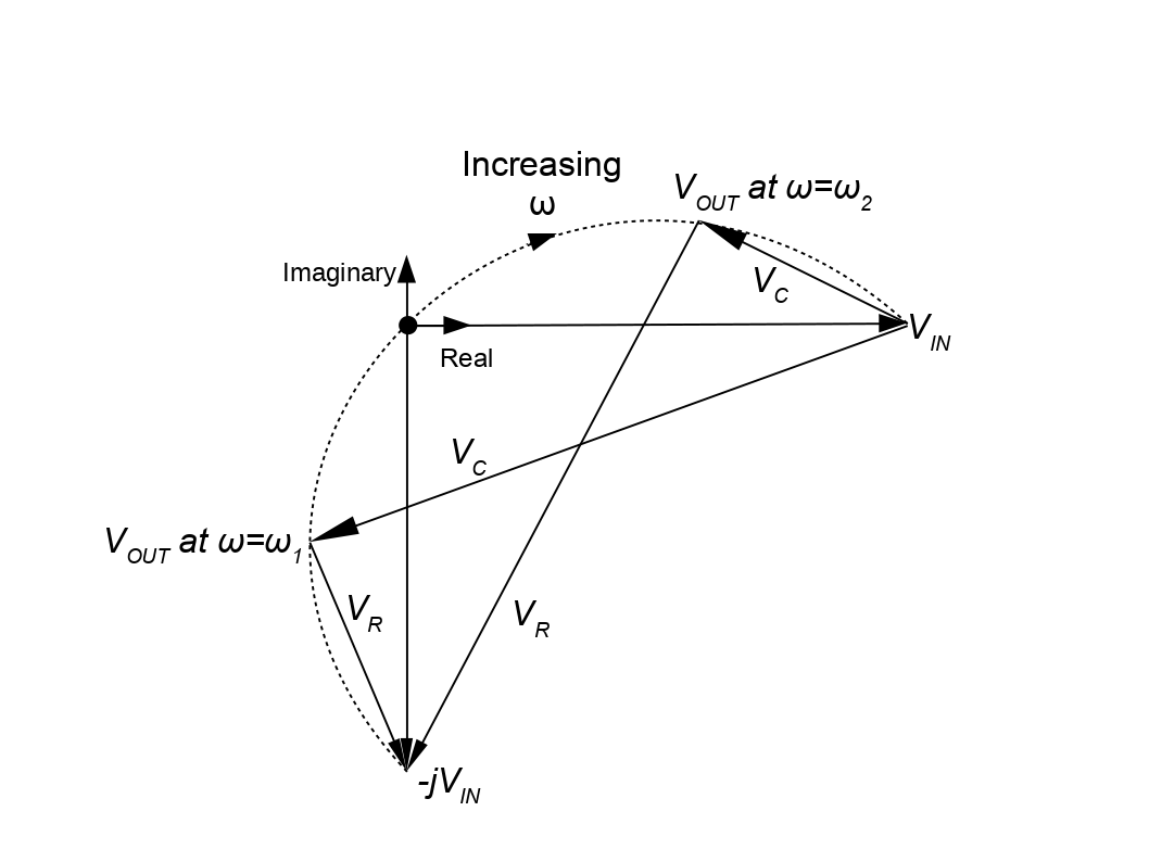
The phasors for VC and VR will still be subject to the same right angle relationship as in the previous network, but the terminal point for the sum of VC and VR will be rotated counterclockwise to the -90 degree direction as seen in Figure 5.
Figure 5. Phasor vector diagram for modified all-pass network
This will stretch counterclockwise the circular dotted line path that the phasor of VOUT traces as the frequency is varied.
From Phasor Diagram to Practical Circuit Network
So we are close to having a network usable in an oscillator, as now the path passes through a point of zero phase shift. However, the geometries work out so that this point will be at the origin of this phasor diagram, which means that as the phase shift passes through zero, the output magnitude will also be zero. This would require an infinite gain to make up by the active feedback loop, so it is clearly an impractical design.
However, Sulzer’s design idea at this point was to add a fraction of VIN with no phase shift to VOUT. Graphically, this would essentially slide the entire dotted path in Figure 5 to the right, so that now the path would cross the real axis to the right of the origin. This means there will be a frequency where the phase through the network is zero at a practical output magnitude for a feedback loop to build up sustained oscillations. The frequency along the path where it crosses the real axis can be tuned by adjusting the single resistance R.
So how did Sulzer translate this abstract phasor diagram into a practical circuit network?
Modern Simulation Tools to Solve Old Challenges
We can now see all the components of the ideal network of Figure 4 in approximate form in the circuit schematic of Figure 1. The voltage divider of R1 and C1 forms at VA an approximation to the -90-degree phase-shifted version of VIN, assuming we are at frequencies greater than the low pass rolloff frequency of this divider, and at an attenuated magnitude. The resistive divider of R2 and R3 forms at VB a version of VIN with no phase shift, and with an attenuation to approximately match that of the R1-C1 divider. The RTUNE-C2 series connection is simply the R and C of the ideal phase shift network. Then the common resistor to ground, R4, will add to VOUT an approximate fraction of VIN by dropping a voltage from VC to ground.
Now that’s a lot of approximation in developing this circuit topology, and Sulzer had to leave his analysis at this fairly rough point in his 1952 article and carry on past this point experimentally. (His graphical phasor analysis actually contains a few errors that I’ve corrected here.)
But by using modern simulation tools and some numerical optimization, we can go beyond his analysis and find the optimum value of the resistor R4 that, due to a fortunate way all the math numerically works out, gives us a network remarkably useful for an oscillator.
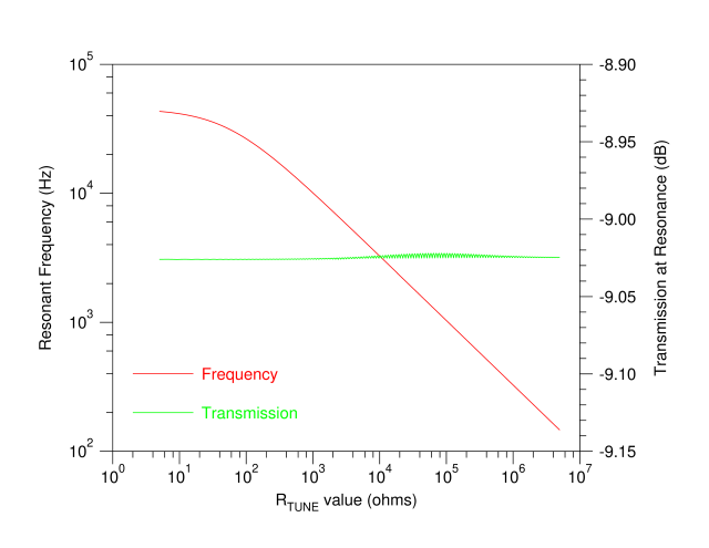
For example, with the component values shown in Figure 1, the value of R4 that optimizes transmission flatness with frequency turns out to be 585 ohms. By running many automated SPICE simulations in a programmed script varying RTUNE and extracting the resonant frequency where the network phase shift passes through zero in each simulation, we end up with the plot shown in Figure 6.
Figure 6. Simulated resonance frequency and transmission of the optimized Sulzer network over RTUNE values with R1=2kΩ C1=100nF R2=2kΩ R3=510Ω C2=5nF R4=585Ω
This plot shows a resonant frequency tuned over two orders of magnitude by varying the single resistor RTUNE through four orders of magnitude, while the transmission amplitude varies only a tiny fraction of a dB! This excellent amplitude flatness over frequency would be very hard to achieve with the mechanically tracking dual tuning components required by classical R-C networks. For most of this characteristic, the oscillation frequency follows the square root of the tuning resistance quite linearly.
You may wonder at this point how critical the value of R4 has to be to achieve this performance.
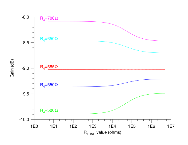
In another fortunate way the math all works out, the optimum for R4 turns out to be fairly broad. The next plot, Figure 7, shows the amplitude flatness with five different values for R4, one the optimum value of 585 ohms and four other values representing large resistor variations.
Figure 7. Simulated transmission through the Sulzer network over RTUNE values for five different R4 values with R1=2kΩ C1=100nF R2=2kΩ R3=510Ω C2=5nF
Even far off from the optimum, the transmission amplitude is still flat to within less than a half a dB, a small enough variation so that whatever amplitude stabilization mechanism used in the overall oscillator, such as the incandescent bulb technique, should easily reduce the output amplitude variation to a very low level.
At a center value of RTUNE, for example 5kΩ, we can take one of the simulation results and look in Figure 8 at the same sort of gain-phase plots as we saw before for the classical networks.
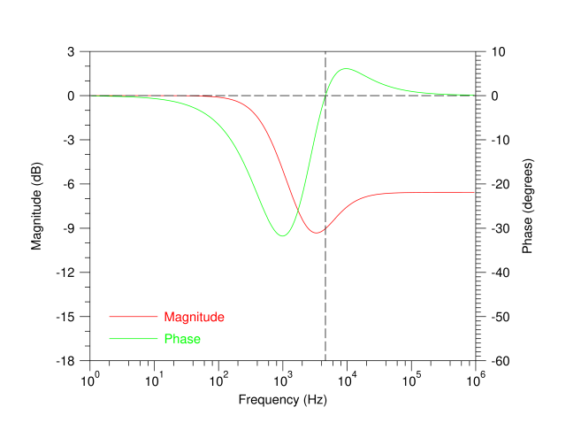
Figure 8. Simulation results for the optimized Sulzer network with R1=2kΩ C1=100nF R2=2kΩ R3=510Ω C2=5nF R4=585Ω RTUNE=5kΩ
At the oscillation frequency where the phase shift passes through zero, the feedback loop gain must make up for a loss of about 9 dB, comparable to that for a Wien oscillator. The overall phase variation shown here is also comparable to that of the Bridged-T network for the typical value of α=4. The magnitude characteristic for the Sulzer network is roughly that of a band-reject filter, so in building a practical oscillator we can use the feedback polarity for the Bridged-T network.
Design Variations
Other choices of the component values in the versatile network of Figure 1 are possible to trade off network attenuation for total tuning range.
For example, raising the values of R1 and R2 from 2kΩ to 4.7kΩ reduces the amplitudes of VA and VB and widens the frequency range over which the -90 degree phase shift approximation is valid.
Running a simulation over a sweep of tuning resistance values now, with a new optimum value of 515 ohms for R4, gives the very wide tuning range seen in Figure 9.
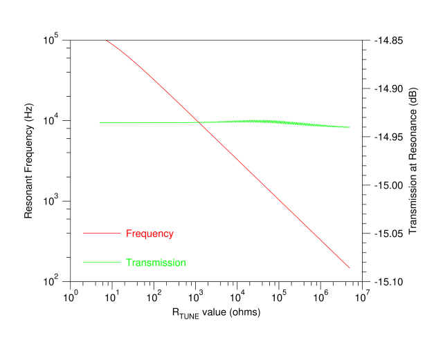
Figure 9. Simulated resonance frequency and transmission of the optimized wide-range Sulzer network over RTUNE values with R1=4.7kΩ C1=100nF R2=4.7kΩ R3=510Ω C2=5nF R4=515Ω
The values of C1=100nF and C2=5nF allow tuning from 150Hz to over 100kHz. Larger capacitor values would allow covering virtually the entire audio range quite linearly in one band, and indeed this sort of oscillator is what Sulzer targeted in his original article. The tradeoff for this wide a frequency range, about three orders of magnitude, is that the attenuation through the Sulzer network has increased to about 15 dB, and requires a higher gain in the active feedback amplifier.
Taking a simulation at the center value of RTUNE=5kΩ shows the deeper attenuation that must be overcome by the gain block in Figure 10.
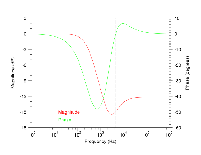
Figure 10. Simulation results for the optimized wide-range Sulzer network with R1=4.7kΩ C1=100nF R2=4.7kΩ R3=510Ω C2=5nF R4=515Ω RTUNE=5kΩ
Potentially this could mean slightly higher distortion, as this greater attenuation takes away from the loop gain that also suppresses any gain nonlinearity.
An Alternative Design
I hope you find Sulzer’s network of enough interest to try it out on a breadboard yourself. The textbook oscillator networks we have used for decades are attractive because they are simple enough to design with analytic derivations and have good phase and attenuation characteristics. Even though Sulzer’s network requires numerical simulation to design effectively, this invention seems to be very valuable for solving the practical tuning problems of the classical R-C oscillator networks.

