In forksheet field-effect transistors (FETs), nFETs and pFETs are integrated into the same structure with a dielectric wall separating them. This approach results in a metal pitch as narrow as 16 nm, which is too low for high-performance cell designs with low track height.
imec researchers highlighted this challenge in their 2022 VLSI paper, introducing a complementary FET (CFET) architecture. They also report how improved process flows make sequential CFETs more promising than monolithic CFETs. Notably, the team posited that this forksheet device architecture might extend the scalability of nanosheet transistor families toward logic nodes 1 nm and beyond.

The evolution from FinFETs to nanosheet to forksheet and finally to CFET.
The Transition From Planar FETs to FinFETs
Thanks to the transition from planar FETs to FinFETs, transistor sizes have decreased while performance has increased. This shift was necessary because the performance of planar FETs began to degrade at reduced gate lengths. FinFETs helped maintain the scaling path.
In a FinFET, the channel between the source and the drain is in the form of a Fin. The gate is wrapped around this channel to exert control from three sides of the channel. This approach eliminates the short-channel effects that planar FETs were suffering. Moreover, higher Fin height allows for a higher device drive current in the same area.
As technology has scaled beyond 5 nm, however, the Fin structure fails to provide enough electrostatic control.
imec's Solution to Scaling Obstacles: The Forksheet Architecture
To enable further scaling, imec has introduced a vertically-stacked nanosheet structure in which the gate fully wraps around the channel. This architecture is said to provide superior control and better distribution of the three-dimensional volume.
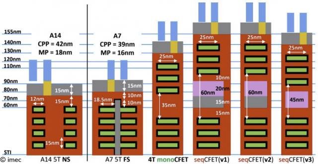
Forksheet devices are an extension of vertically-stacked nanosheets. Here, the nanosheets are controlled by a tri-gate forked structure, which is achieved by introducing a dielectric wall between the p and nFET devices. The isolation allows for tighter n-to-p spacing and higher performance. The isolation also extends the standard cells to 4T in track height, meaning that four intracell metal lines can fit in the range of the standard cell height.
However, the spacing between the n- and p-region of the metal pitch is as low as 16 nm, which is too narrow for 4T track height cell designs. To maximize the channel width and the drive current, imec researchers proposed the CFET architecture.
Monolithic vs. Sequential Complementary FETs
Researchers explore two possible integration schemes to enable vertical stacking: monolithic and sequential. In a CFET architecture, n- and p-devices are stacked on top of each other vertically, eliminating the n-p spacing from the standard cell height.

Gate cross sections for nanosheet, forksheet (FS), and CFET (monolithic and sequential).
A monolithic CFET flow occurs in three parts: epitaxial growth of a bottom channel, deposition of an intermediate layer, and then the epitaxial growth of a top channel. This flow is more complex than a sequential flow because it results in high aspect ratio (HAR) vertical structures, requiring further patterning.
In the sequential fabrication flow, the bottom devices are processed up to the contacts. Then, a blanket semiconductor layer is created on top of it using wafer-to-wafer bonding techniques. Finally, the top device is integrated. This process is simpler because top devices can be processed separately in a two-dimensional way.

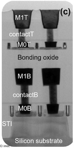
3D sequentially stacked devices.
Each of these processes has its advantages and disadvantages. In their 2022 VLSI paper, imec researchers presented a power-performance-area-cost (PPAC) evaluation of monolithic CFETs versus sequential CFETs in a 4T standard cell design. They also evaluated different layer transfer processes for the sequential CFET.
From Theory to Implementation
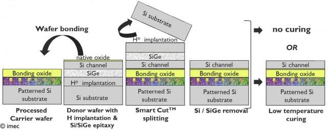
imec reported that from a cost perspective, semiconductor manufacturer SOITEC offers a promising layer transfer process—one that relies on a low-temperature "Smart Cut" flow. It uses an engineered bulk donor wafer that splits at low temperatures. The researchers found that top-layer devices processed after the proof-of-concept layer transfer recovered from degraded electrical performance.

Illustration of the SOITEC low-temperature Smart Cut layer transfer flow.
Naoto Horiguchi, director of the logic CMOS scaling program at imec, emphasized that while this architecture is a true CFET architecture, it is not a true CFET implementation because the metal interconnect layer is absent from the bottom device.
He notes that imec's test vehicle demonstrated "improved layer transfer as a key module for sequential CFET and other 3D sequential stacking implementations." In future studies, imec reported, researchers will work toward true sequential CFET implementation.
All images used courtesy of imec
