Last week, Cadence announced the release of an "industry’s first:" a comprehensive platform called Integrity 3D-IC. The platform is said to bring together workflows facilitating system planning, co-design with other Cadence platforms, and system-level analysis and sign-off of 3D advanced packaging for chiplet-based system-on-chip (SoC) designs.
A trending fabrication method to overcome limitations in Moore’s Law scaling is to stack chiplets in 2.5D and 3D configurations to form a vertically integrated SoC. “More than Moore” expresses the need to move beyond node scaling to facilitate improvements in power, performance, and area (PPA).
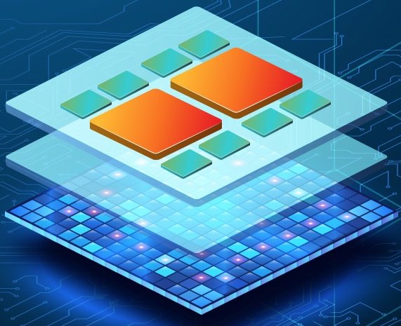
Utilizing chiplet modularity in 3D design.
Moving from complex advanced nodes to more cost-advantaged modular IP-chiplets requires ECAD capabilities to support analysis in thermal management, power requirements, and inter-chiplet timing constraints.
The Industry Needs 3D-IC Design-System Analysis
The Integrity 3D-IC platform is a timely addition to the ECAD ecosystem. The industry is approaching a time where the cost of monolithic SoC designs is increasing exponentially, which is pushing the NRE costs beyond the recovery point.
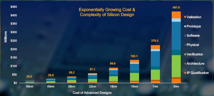
Cost is limiting the return on design investment.
High expenses and advanced package technology have given rise to a need for a 3D IC workflow. This platform must be capable of a complete package and system analysis of thermal, power, and static timing metrics.
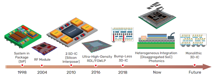
20-year evolution of advanced package technologies.
Introducing the Cadence Integrity 3D-IC Platform
The current paradigm for stacked SoC technology is based on the heterogeneous integration of chiplets. Chiplets are small IP blocks with standardized interfaces designed to be dropped into a larger system-on-chip device.
3D integrated circuits are interconnected by Through Silicon Via (TSV) technology, microbumps, and interposers to elevate performance and reduce power requirements while maintaining or reducing system area.
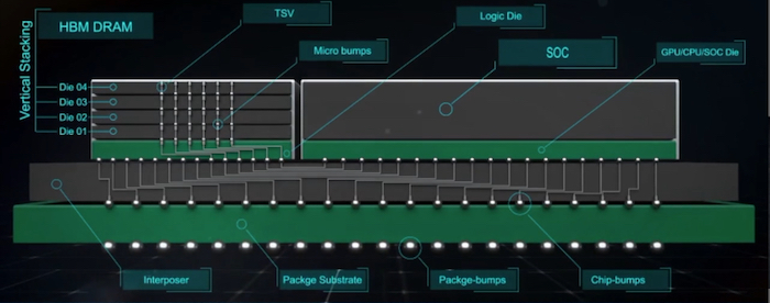
Example of a 3D integrated circuit.
Cadence Integrity 3D-IC is said to be a single-cockpit, high-capacity ECAD for the design, planning, analysis, and verification of stacked 3D chips. The platform supports multiple advanced packaging configurations including fan-out wafer level packaging (FOWLP), RDL and silicon interposer, wafer on wafer/wafer on-chip, and 3D stacking.
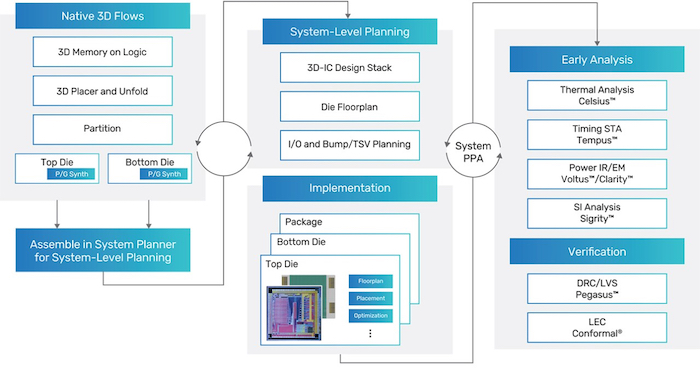
The Cadence Integrity 3D-IC workflow.
Integrity 3D-IC is intended to bring a host of system-driven PPA closure features under one ECAD suite including a native TCL database, co-design for digital and analog/RF chiplets, native 3D stacking, and advanced routing.
Central to the seamless workflow of Integrity 3D-IC is a hierarchical database that is said to support multiple technology files from different design nodes. This database is an extension of Innovus database, and this allows the 3D-IC database to support a digital die hierarchical design.
Integrity 3D-IC Platform's Verification and Analysis
The thermal design of stacked-IC technology is far more complex than a traditional planar die. This is because the chiplets are further removed from the largest heat sink in the overall system (the PCB) and various chiplets have dissimilar thermal profiles.
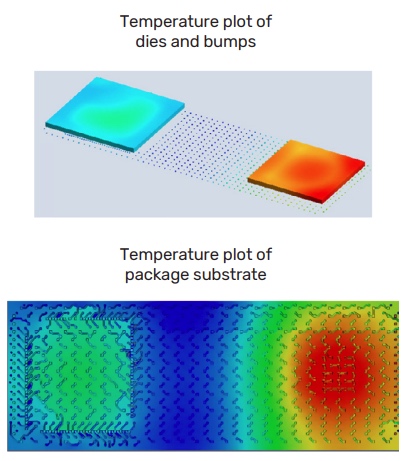
Thermal analysis of two chiplets.
Using the finite element analysis (FEA) and a computational fluid dynamics (CFD) engine capabilities of the Cadence Celsius Thermal Solver, engineers designing a 3D stacked IC can account for transient and steady-state thermal considerations including the conduction analysis for bumps and bonding wires.
Moving beyond thermal considerations, Integrity 3D-IC can perform early rail analysis to optimize the system power delivery networks (PDNs), provide multi-die static timing validation, and ensure inter-die connectivity with design rule checks for physical connectivity.
3D ICs Forge Ahead to Beat Moore's Law
The key aspect to Integrity 3D-IC is its position inside the suite of solutions offered by Cadence. By providing a common cockpit and database for an entire suite of planning and validation solutions, Cadence has positioned itself well in the ECAD market for advanced 3D design.
3D IC paradigms add complexity to SoC design in a way that is different from traditional planar die-on substrate design. The benefit of vertical integration of IP blocks allows for shorter interconnects and lower power requirements along with increased system performance.
Chiplets provide a system of modularity for IP blocks, which allows fabricators to spread the cost of IP design and validation over a series of stacked-IC applications instead of being limited to a single monolithic SoC.
All images used courtesy of Cadence.
