Nick Holonyak Jr., the inventor of the first visible-spectrum LED, passed away on September 18 at age 93, leaving behind a rich legacy of research work in semiconductor devices, plasma science, photonics, and optoelectronics.
LEDs are everywhere and it is difficult to imagine a world without them. Creating a mood with dimmed light switches, enjoying our favorite music played by DVD laser diodes, LCD TVs, and having super-fast fiber optic Internet are just some of the modern-day’s conveniences that are a result of LED technology made possible by Holonyak.
A Mentor at University of Illinois
Holonyak spent his last years before retirement in 2013 as John Bardeen Endowed Chair Emeritus in Electrical and Computer Engineering and Physics at the University of Illinois.
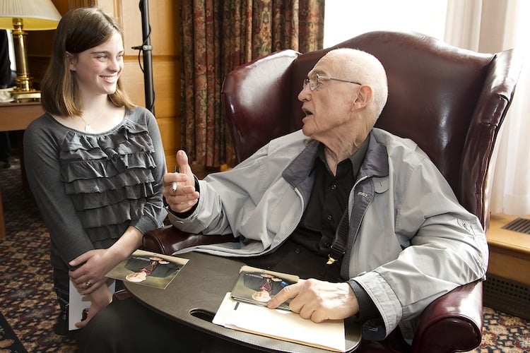
Nick Hollonyak Jr. in his mentorship role talks to a University of Illinois student on the occasion of the 50th anniversary of the LED in 2012. Image used courtesy of L. Brian Stauffer via Univ. of Illinois
At this timely moment, we remember how Nick Holonyak’s stubborn, yet clever work on three-component GaAsP (Gallium Arsenide Phosphide) alloys illuminated the diode, which, up until October 9, 1962, was based on infrared radiation and beyond the range perceivable to human eyesight.
Nick Holonyak Jr. was born in 1928, in Zeigler, Illinois. His father, a coal miner, was an Eastern-European immigrant from what is today’s Ukraine. Initially, Holonyak followed his family pathways and started earning his wages as a railroader.
But having the knack to build literally any tool by himself, he took a chance; he used his three-year savings from working as a physical laborer on the railroad to finance his studies in electrical engineering at a nearby college. Excelling in electronics, he later enrolled in the University of Illinois (UI), where he received all three degrees: B.S. (1950), M.S. (1951), and a Ph.D. (1954).
Mentored by John Bardeen
At the university, he had the luck to meet John Bardeen, the only engineer to be awarded the Nobel Prize for physics twice, once for the invention of the transistor, and the second time for the microscopic theory of conductivity. Holonyak was Bargeen’s first graduate student and collaborated with him until his death in 1991.
In 1963 Holonyak became a professor at the University of Illinois, where he worked for 50 years. He was tireless as a professor, researcher, and mentor, having made numerous contributions alongside his fellow colleagues.
Quantum Well Laser and Transistor Laser
The quantum-well laser used for material processing, medical therapy, diagnostic devices, and laser printing was a joint project between Holonyak and his students.
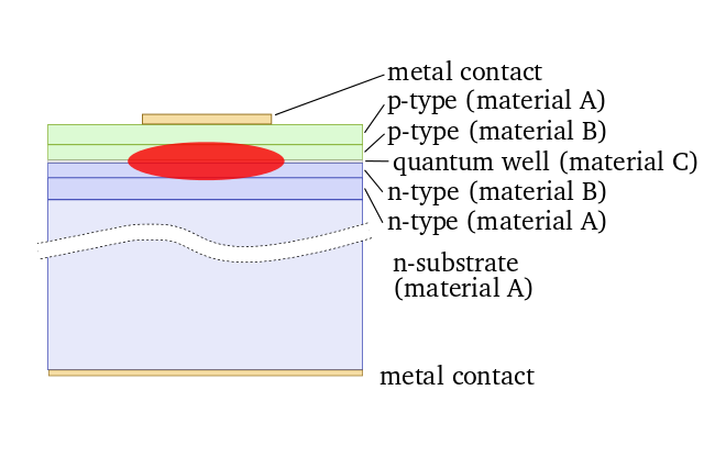
A simple demonstration of a quantum-well laser diode. Image used courtesy of Wikimedia Commons
Holonyak also made his mark in optical data transmission by “bending light” in GaAs (gallium arsenide) chips.
With Milton Feng, a fellow Illinois professor, Holonyak invented the transistor laser, a special type of three-terminal photonic transistor with both electricity and light output signals. The work was presented to the public in a conveniently named paper “The Metamorphosis of the Transistor into a Laser”.
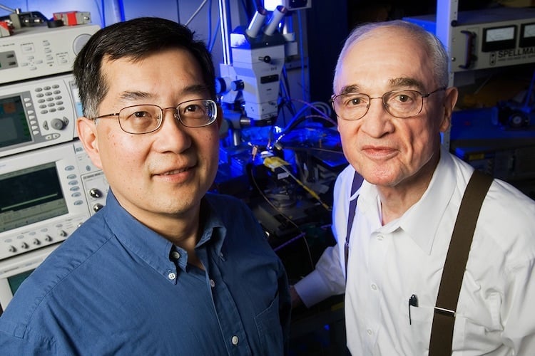
Milton Feng (left) and Nick Holonyak (right) frequently worked together. Image use courtesy of University of Illinois
Earlier in his career at GE, he made the first silicon tunnel diodes and researched photon-assisted tunneling.
The First Red LED
This month marks the 60-year anniversary of the red light-emitting diode (LED), which paved the way for the full-spectrum lights and lasers now used in home lighting, medical devices, and consumer electronics. And Holonyak was there at the beginning.
For a year after graduation from the University of Illinois, Holonyak worked at Bell Telephone Labs. From 1955 to 1957 he worked in the military, in the U.S. Army Signal Corps. He did his most significant work in General Electric, in the GE Advanced Semiconductor Laboratory in Syracuse, which, at the time, heavily invested in researching optoelectronics.
Apart from Holonyak, Robert Noel Hall also worked on LEDs in the GE Schenectady lab although he used different methods (polishing) and materials (GaAs), which eventually got him the credit for successfully operating the first infrared semiconductor laser.
In a way, he managed to beat Holonyak, an accomplishment which the LED inventor acknowledged himself. How did this happen? Hall succeeded in creating the laser cavity before Holonyak.
The laser cavity is a region on the material that serves as a gateway for light waves to travel back and forth and generate additional radiation. Instead of using cleaving as Holonyak did, Hall polished the opposite faces of the GaAs crystals. However, Holonyak is recognized as the inventor of LED because he was the first one to place lasers in the visibility spectrum.
Three-element GaAsP Alloy
At odds with fellow chemists, Holonyak decided to illuminate the GaAs diode by adding a third element to it, phosphorus, developing a three-element crystal alloy gallium arsenide-phosphide (GaAsP).
Those opposing his efforts argued that alloys are unstable and could not produce coherent light. But he stuck to his views. The idea behind his conviction emerged from his understanding of the electron’s ability to jump from orbits further from the nucleus to an electron-free orbit closer to the nucleus when excited by an electric charge.
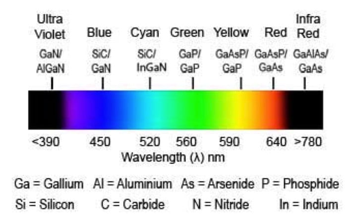
Combinations of semiconductor materials used to produce different colors. Image used courtesy of Learn About Electronics
Apart from borrowing some of Hall’s methods, Holonyak considered other aspects of the LED laser a product of teamwork.
He spoke of the importance of Maiman’s research on the ruby rod laser and of J.C. Marinace of IBM, who used heated iodide gas to transport germanium from a hot to a cooler place in a tube and deposit it on a seed germanium crystal. Holonyak replicated the procedure by using heated chlorine.
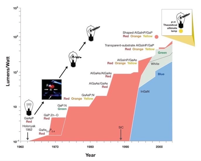
The “Alloy Road”—the evolution of the LED alloys. Image used courtesy of Springer
The LED he originally made was a tiny diode that generated weak red light. It took several more years for researchers to explore alternative materials and add blue and green light so that the full spectrum of white light could be produced.
Unlike the original LED, today’s LEDs are fabricated in many shapes, depending on the application. LED lights are usually small diodes made out of a semiconductor material that is grown in high-pressure chambers to produce a crystal ingot. The ingot is then cut into wafers, purified, and improved with dopants to create various lights. The metal wiring and the plastic packaging come at the end.
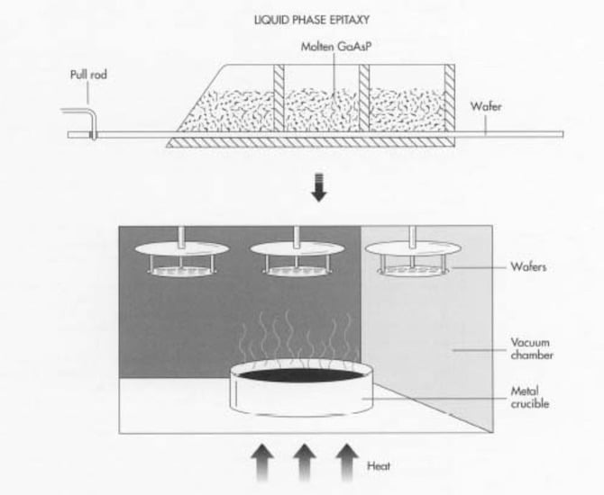
The process called Liquid Phase Epitaxy is used for adding additional crystal layers on the wafer surface. Image used courtesy of How Products Are Made
Nick Holonyak had a long list of awards and titles for his outstanding achievements in academia and research, including the Edison Medal of the IEEE, the National Medal of Science, the Japan Prize, the IEEE Third Millennium Medal, the IEEE Medal of Honor (2003), and the Lemelson-MIT Prize (2004).
Holonyak was a member of the National Academy of Sciences (NAS), the National Academy of Engineering (NAE), a fellow of the American Academy of Arts and Sciences, a fellow of the American Physical Society (APS), a foreign member of the Russian Academy of Sciences (RAS), and a life member of the Institute of Electrical and Electronics Engineers (IEEE).
Lead image used courtesy of University of Illinois News Bureau