Since 2017, Samsung has held an annual “Tech Day” conference, where the company releases new technology, discusses the state of the industry, and unveils its plans for the future. At Tech Day 2022, which took place on the heels of Foundry Forum 2022, Samsung laid out plans for its upcoming 1.4nm process node, memory roadmap, and goals to expand its industry outreach. In this article, we’ll discuss some of the major highlights of the conference.
Samsung Looks to 1.4nm
At Samsung's Foundry Forum 2022, the company announced plans to continue scaling its process technology. Earlier this year, Samsung began production of its 3nm node—the first foundry in the industry to accomplish this feat. Now, Samsung has set its sights on next-generation process technology, specifically a 2nm node.
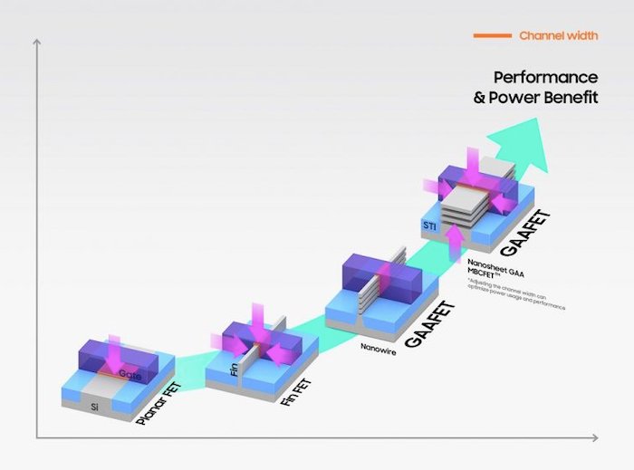
MOSFET evolution to reach advanced nodes. Image courtesy of Samsung
Samsung plans to reach 2nm production by 2025. Achieving this scale will require Samsung's gate-all-around (GAA)-based transistor technology. Beyond that, the company envisions reaching the 1.4nm node by 2027 and aims to triple its advanced node production in the same year.
Big V-NAND and DRAM Plans in the Works
Samsung also unveiled its eighth- and ninth-generation V-NAND offerings and its fifth-generation DRAM offerings.
The company currently offers 512 Gb triple-level cell (TLC) products for V-NAND but anticipates releasing a 1 terabyte TLC version later this year. The fifth-generation DRAM offering will be a 10nm (1b) device and will enter mass production in 2023. Other DRAM solutions coming soon include a 32 Gb DDR5 solution, 8.5 Gbps LPDDR5X DRAM, and 36 Gbps GDDR7 DRAM.
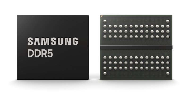
A rendering of Samsung’s newest DDR5 solution. Image courtesy of Samsung
Samsung has big plans for its V-NAND, claiming that by 2030, it will achieve a 1,000-layer V-NAND. To reach this goal, Samsung is transitioning from its current TLC architecture to a quad-level cell (QLC) architecture, increasing density and enabling more layers.
Samsung will also invest more resources into DRAM R&D, researching new architectures and materials, such as High-K, to help scale DRAM beyond 10nm. The company intends to further develop other DRAM solutions, such as processing in memory (PIM).
Samsung Collaborates Across the Industry
Samsung used Tech Day 2022 as an opportunity to lay out some of its plans for industry outreach.
Samsung’s System LSI Business announced its intention to become “total solution fabless.” By this, the group means that it will leverage its product offerings, including SoCs, PMICs, and security solutions, into a single platform to be leveraged by its customers. This way, Samsung can design custom solutions for its customers without a fab.
Samsung is also increasing its industry outreach by expanding trade partnerships. Specifically, the company will be opening a Samsung Memory Research Center (SMRC), where customers and vendors can test Samsung memory devices in various applications and environments. This center will be designed in collaboration with partners, including Red Hat and Google.