As semiconductors have continued to shrink, the industry has faced several outstanding design and manufacturing challenges. One of these challenges is meeting the necessary doping concentrations of Group V elements in silicon wafers.
TSMC has previously predicted that these challenges could be solved using microwaves, but to this point, no researchers have successfully implemented this technique. Last week, researchers from Cornell University affiliated with TSMC published a new study describing the first successful use of microwaves for semiconductor doping.
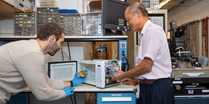
Dr. James Hwang (right) and Gianluca Fabi with their modified microwave oven. Image (modified) courtesy of Ryan Young/Cornell University
In this article, we’ll discuss the existing challenges with semiconductor doping, TSMC’s microwave theory, and the new research from Cornell.
The Challenges of Semiconductor Doping
Material doping is the process of selectively adding atoms of foreign material into the crystal lattice of silicon to change the material’s electrical properties. For n-type doping, silicon is doped with a Group V element such as phosphorus, while p-type doping uses Group III elements such as boron or gallium.
Historically, doping is achieved through a process known as ion implantation. Ion implantation is a low-temperature process in which dopant atoms enter the crystal lattice of silicon and come to rest at some depth within the solid. The wafer then undergoes a thermal annealing “activation” process, in which the wafer is heated and cooled to repair any residual damage to the lattice.
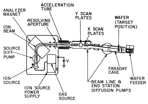
Schematic of an ion implanter. Image courtesy of the City University of Hong Kong
However, as semiconductor nodes shrink, several issues plague this traditional process—one being a higher concentration of free electrons to maintain the same electrical performance. At today’s semiconductor sizes, the required free-electron concentration of phosphorous, for example, is currently higher than the phosphorous’ equilibrium solubility in silicon.
Additionally, as transistors take on new architectures such as 3D nanowire and nanosheet MOSFETs, traditional thermal annealing techniques are no longer effective because the high annealing temperatures create vacancies in the material's surface.
Cornell Professor Finds a Path Forward With a Modified Microwave
To address these problems, engineers from TSMC theorized an activation process using microwaves to activate the excess dopants. To test this theory, TSMC teamed up with researchers from Cornell University—led by research professor Dr. James Hwang—to develop a modified microwave oven that selectively controls the activation of dopants in a silicon crystal. Instead of producing a random standing wave pattern (as microwave ovens do in normal operation), the researchers' microwave controls the location of where the standing waves occur.
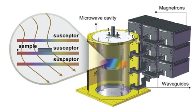
Setup of the microwave annealer. Image courtesy of ResearchGate
With this modified microwave oven, Dr. Hwang's team achieved high precision in their activation process without overheating the silicon crystal, avoiding damage and surface vacancies as a result. The researchers used a 12 kW microwave at 2.45 GHz to produce a 30-nm-thick Si nano-sheet that was doped with 3 x 1021 cm-3 of phosphorus in six minutes. The resulting wafer had a free-electron concentration of 4 x 1020 cm-3 and a stable doping profile with less than 4% variation.
How Microwave Annealing May Extend Moore's Law
Through this research, Dr. Hwang and his fellow researchers proved TSMC’s theory that microwave annealing can indeed result in efficient activation and thermal stability. According to the team, this work may enable scaling beyond 2nm. Beyond this, the researchers cite the potential of this breakthrough to make way for new transistor architectures in which horizontally-stacked nanosheets can further increase the density and control of transistors.
Dr. Hwang and postdoctoral researcher Gianluca Fabi, who have jointly filed two patents for the prototype microwave annealer, say their findings could be used to develop semiconductor materials and electronics as soon as 2025.