At its GTC event back in March, NVIDIA introduced a set of new technologies such as their Grace CPU, Hopper GPU, and NVLINK-C2C interconnect architecture.
Now NVIDIA is giving us more in-depth information and technical detail about these releases. At this week’s Hot Chips 34 conference, a number of NVIDIA speakers took the stage, each providing the industry with more insight into what makes each of these releases so special.
In this article, we’ll be looking at some of the exciting details released for each of NVIDIA’s new flagship technologies.
Grace CPU and Cache Coherency
One of the most exciting releases that came from NVIDIA this year was their Grace CPU “Super chip.” In this week’s presentation, NVIDIA Jonathon Evans, Distinguished Engineer at NVIDIA, took the stage to reveal more detail about the super chip.

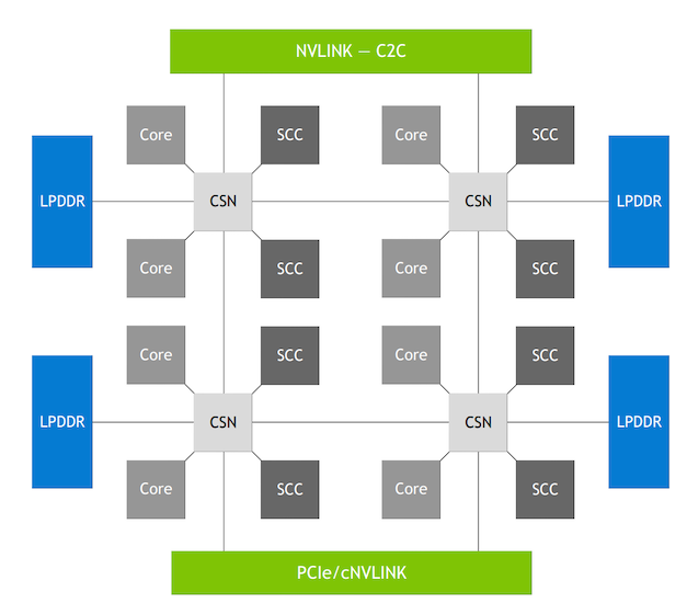
NVIDIA’s Scalable Coherency Fabric (SCF). Image used courtesy of NVIDIA
Grace was designed for data center computing, and specifically AI processing, while optimizing power consumption and performance on the device and system level. As discussed in the presentation, Within this pursuit, one of the most important aspects of Grace was the use of NVIDIA’s Scalable Coherency Fabric (SCF).
The SCF is a mesh interconnect architecture that connects NVIDIA fabric and distributed cache design. Specifically, the SCF is meant to connect different internal subsystems within the Grace CPU, including memory, CPU cores, and I/O. To achieve this, NVIDIA tells us that SCF can achieve a bi-section bandwidth of 2,335.6 GB/s, supporting up to 117 MB of L3 cache, and scalable up to 72+ cores.
Beyond this, SCF offers a number of useful functions such as featuring the Arm standard for partitioning system resources. With this standard, Grace can assign partition IDs to each entity requesting memory, and SCF cache resources can be partitioned between the different IDs. Specifically, SCF can partition cache capacity and memory bandwidth, while performance monitor groups monitor resource usage.
Hopper GPU: Streaming Multiprocessor
Moving beyond Grace, NVIDIA’s Jack Choquette, CPU and System Architect, gave a presentation that shed light on some technical details of the Hopper GPU.
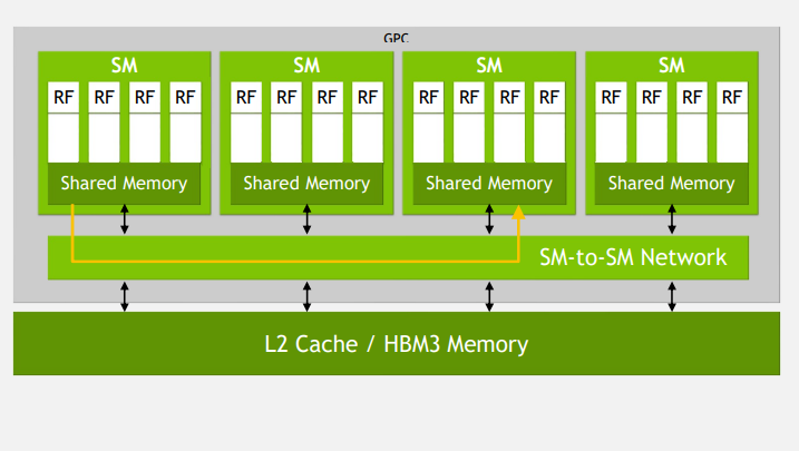
One of the key points of Choquette’s talk was about Hopper’s new streaming multiprocessor (SM) architecture. In Hopper, NVIDIA is introducing a new component that it calls the “SM to SM Network”, which is a high-bandwidth communications fabric that connects resources within Hopper's graphics processing cluster.
The idea is to allow for streaming multiprocessors to communicate directly without requiring access to memory. This significantly decreases latency for the processing cluster, resulting in 2x faster FP32 and FP64 FMA, and also supports up to a 256 KB L1 cache.

Hopper’s SM-to-SM Network. Image used courtesy of NVIDIA
Beyond this, the talk covered a number of interesting and important concepts that guided the design of Hopper.
A large theme of the conversation centered around how NVIDIA aimed to exploit spatial and temporal locality, where gridded architectures and threaded blocks help NVIDIA’s CUDA to achieve decreased latency and greater parallel performance.
Other concepts include NVIDIA’s use of Hopper as an asynchronous GPU, allowing for improved performance by allowing threads to execute at different rates from one another. This offers large benefits in performance as idle time is minimized so that each unit is fully utilized and parallel computation can be optimized.
NVLink for Chip-to-Chip Integration
Finally, a key building block of the Hopper architecture was the introduction of the NVLink-C2C interconnect technology. In a talk by NVIDIA system architects Alexander Ishii and Ryan Wells, NVLink’s importance was further discussed.
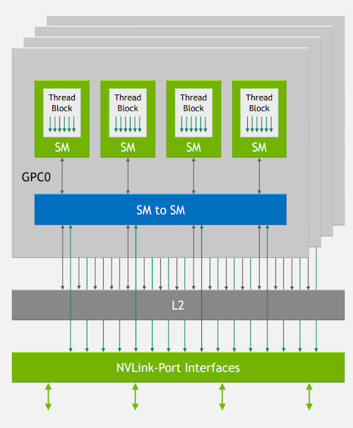
NVIDIA’s idea for designers is to develop computing platforms that will leverage hundreds of Hopper GPUs in one cluster, and to achieve this will require a high-speed device-to-device interconnect. For Hopper, that interconnect is NVLink-C2C, and, according to the talk, the main benefits are a faster rate than PCIe (100 Gbps-per-lane vs 23 Gbps-per-lane), as well as lower overheads than a traditional network.

NVLink-Port Interfaces are a crucial aspect of the Hopper architecture. Image used courtesy of NVIDIA
For example, NVIDIA’s turnkey AI HPC data center solution is a large computing cluster called SuperPOD. In the SuperPOD architecture, one can find 32 DGX H100 servers and 18 NVLink Switches which provide 56.7 TB/s NVLink Network bisection bandwidth and can provide up to 1 ExaFLOP of AI performance. According to NVIDIA, this performance is only made possible thanks to the NVLink interconnect technology.
