The boost converter is a DC-DC converter used to create an output voltage that is higher than the input voltage. Boost converters are also used to drive LEDs placed in series in products like LED flashlights. The boost converter suffers from vulnerability to a short circuit load. This paper discusses why boost converters are vulnerable to short circuits, ways to protect a boost converter from short circuit, and alternative power electronics converters that don’t have a short circuit vulnerability that can be used in place of the boost converter.
Intro to the Boost Converter
As previously stated, a boost converter produces an output voltage that is higher than the input voltage. Examples of boost converters include the following:
- Producing 5V charging ports in a lithium battery pack
- Producing power rails in a smartphone.
- Driving LEDs in series in an LED lantern or flashlight.
- A voltage regulator in an Arduino-based project.
- Creating a high voltage to run a motor from a single cell lithium battery.
Figure 1 is a simplified schematic of a boost converter. It’s a simple circuit constructed of capacitors, an inductor, a MOSFET, and a diode. The output is controlled through a closed feedback loop (not shown for simplicity's sake) by controlling the duty cycle, or percentage of time that the MOSFET is on. The transfer function, or ratio between output voltage and input voltage is $Vout/Vin = 1/(1-D), where Vout is the output voltage, Vin is the input voltage, and D is the duty cycle. A real boost converter would have a PWM controller chip, which is not shown in figure 1.
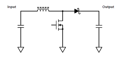
Figure 1: Simplified schematic of a boost converter
Notice that if the output terminal of the boost converter is short-circuited to ground, then the input voltage is shorted to ground through the inductor and the diode. There is nothing limiting the current that will flow except wire resistance, and the current limit of the power source attached to the input voltage. The boost converter will fail with the diode, inductor, or traces catching on fire, melting, or some other sort of catastrophic failure if steps are not taken to protect the boost converter.
General Protection Strategy
The general protection strategy outlined in this paper is to introduce a switch in between the power source and the boost converter that is used to disconnect the boost converter from the power source in the event of a short circuit load condition. This switch can be realized as a MOSFET, a load switch, a boost converter integrated circuit with a built-in protection switch, or a fuse.
Protection with a MOSFET
A MOSFET added to the front of the boost converter can be used to disconnect the power source from the boost converter. See figures 2 and 3 for simplified schematics. The MOSFET may require additional circuitry to bias the gate. An n-channel MOSFET requires its gate voltage to be higher than its source terminal. This may require a gate driver IC or a charge pump.. A p-channel MOSFET requires that the gate is pulled below its source terminal. If the input voltage is sufficiently high, the gate of a p-channel MOSFET can be pulled to ground to turn the MOSFET on. For this reason, using a p-channel MOSFET may be the simplest and easiest choice. Notice that in both schematics the MOSFET body diode points from the boost converter to the power source so that current is blocked, unless the MOSFET is turned on.
When choosing a MOSFET for this application, the drain-source voltage rating, RDS(ON), and gate voltage threshold are important figures to consider. The drain-source voltage rating should be a few voltages higher than the maximum input voltage. The on-state resistance should be low enough to not generate many $P=I2R$ losses. The gate threshold voltage should be low enough that the MOSFET can be easily turned on and off.
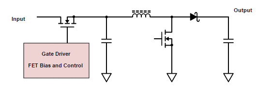
Figure 2: Simplified schematic of a boost converter with an n-channel MOSFET between the power source and boost converter input for short circuit protection.

Figure 3: Simplified schematic of a boost converter with a p-channel MOSFET between the power source and boost converter input for short circuit protection.
Protection with a Load Switch
A load switch is power MOSFET with additional circuitry integrated. Additional features may include a charge pump and level shifter to bias the MOSFET gate and also overcurrent protection features that shut the switch off if current is excessive. Using a load switch has the following advantages over using a MOSFET:
- Reduces BOM count
- Reduces PCB footprint
- Reduces the complexity of design, as you don’t have to add additional control circuitry.
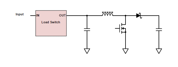
Figure 4: Simplified schematic of a boost converter with a load switch on the input for short circuit protection.
Boost Converter Controllers with Built-in Protection
Practical boost converters are controlled by an integrated circuit that regulates power conversion. Some of these boost converter controller circuits have built-in protection mechanisms such as load switches. Using a controller with built-in protection simplifies design, reduces BOM count, and reduces PCB footprint. Examples of boost converter IC’s that include protection features are Texas Instruments’ LM4510 and TPS61080.

Figure 5: Simplified Example of a Boost Converter IC with Built-in Protection
Protection with Fuse
A fuse can be placed on the input or output of a boost converter to protect against short circuit load conditions. See figure 6 for an example of how this is done.
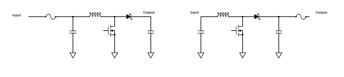
Figure 6: Protection with Fuses on Input or Output of Boost Converter. Note that load switches and MOSFET protection circuits can also be placed between the boost converter output and the load, as is pictured with the fuse protection circuits.
The author recommends using the other approaches outlined in this article because the design with a fuse is more troublesome. If a short circuit condition occurs, the fuse will blow and have to be replaced. Circuits built with extra protection MOSFETs, load switches, or integrated protection will not require any components to be replaced if the converters work properly. These designs will save the end user the time and money of replacing burned fuses. Additionally, fuses do not trip as quickly as one would expect from reading the datasheet. This can result in components and traces being burned up before the fuse blows. Designs using MOSFETs, load switches, and ICs with integrated protection can disconnect from loads in microseconds or faster, providing extra safety and robustness for the circuit. However, the fuse solution may be the simplest and cheapest to implement.
Conclusion
The boost converter is used everywhere but suffers from vulnerability to short circuit loads. This paper has discussed several approaches to getting around this vulnerability including using MOSFETs, load switches, ICs with built-in protection, and fuses to disconnect the power converter in the event of a short circuit condition.