Moore’s law, the observation that the number of transistors in a single integrated circuit doubles every two years, has been the backbone of the semiconductor industry since its inception. Using the same traditional CMOS transistor architecture, the semiconductor has relied on device scaling to achieve Moore’s law—but in 2021, we are quickly reaching an impasse.
Transistors have gotten so small that traditional device scaling no longer applies; the result is that Moore’s law is fundamentally threatened. To overcome this challenge, researchers have been exploring new ways to develop semiconductors—focusing on anything from fabrication to material to architecture.

Depiction of the evolution of transistor architecture. Image from Sheng-Kai Su et al.
This week, IBM, in collaboration with Samsung, announced the VTFET, a new transistor architecture they believe will breathe new life into Moore’s law.
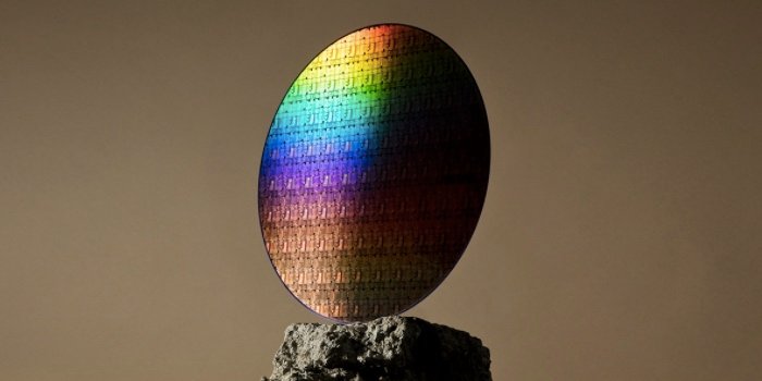
Wafer for a VTFET. Image used courtesy of IBM
Lateral Transistors and Scaling Challenges
The traditional CMOS architecture and the FinFET architecture that is used in almost all electronic devices today make use of a lateral transistor architecture.
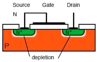
Semiconductor architecture of a lateral MOSFET.
In this setup, current flows from drain to source (NMOS) laterally across the induced channel of the FET. Historically, device scaling involved decreasing the length of the transistor’s channel, which resulted in lower channel resistances and hence more current flow at the same voltage levels or, importantly, the same current flow at lower voltages.
As FinFETs were introduced and devices grew smaller, designers began concerning themselves with a new, more telling metric called contacted gate pitch (CGP). CGP refers to the minimum distance from one transistor's gate to another and is functionally an indicator of the physical space where all components fit.
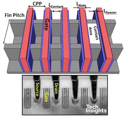
Contacted gate pitch for a FinFET. Image from Razavieh et al.
Today, lateral transistors at the nanosheet level have reached a point where researchers can no longer scale down traditional devices due to challenges such as tunneling and fabrication. As a result, designers are forced to trade off parameters such as the gate, spacer, and contact size, which negatively impacts performance and power. Lateral transistors are essentially reaching the CGP limit, making it nearly impossible to increase device density with lateral transistors.
What is a VTFET?
To address scaling barriers posed by lateral MOSFETs, IBM and Samsung announced the vertical-transport nanosheet field-effect transistor (VTFET).
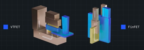
The VTFET is aligned vertically as opposed to the lateral FinFET. Screenshot from IBM
In contrast to traditional lateral transistors, the VTFET architecture layers transistors perpendicular to the silicon wafer and induces a flow of current vertically to the surface of the wafer. The main benefit of this vertical orientation is that the device’s gates, spaces, and contacts are not constrained in traditional ways, allowing more freedom to optimize designs and increase CGP without sacrificing performance.
With less stringent constraints than lateral transistors, VTFETs can then employ larger source/drain contacts than otherwise possible to increase a device’s current driving capacity. Further, VTFETs allow designers to optimize their design between drive current, leakage, and capacitance to improve switching speeds or power use.
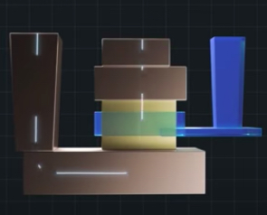
Profile view of a VTFET. Screenshot from IBM
According to IBM, VTFETs can pave the way for Moore’s law scaling beyond the nanosheet technology in CMOS design. IBM predicts that with advanced nodes, the VTFET architecture could enable double the performance or up to 85% reduction in power consumption compared to FinFETs.
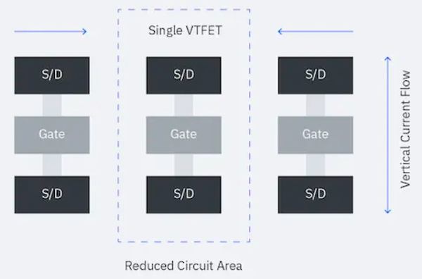
Configuration of the new VFET. Image from IBM
Beyond Moore's Law
With traditional Moore’s law approaching an end, researchers have looked for a solution that may revitalize device scaling. IBM and Samsung believe to have found a solution in the VTFET, which they think holds promise for significant improvements in power, performance, and size over traditional FinFETs.
