The struggle to fit more and more technology into an ever-decreasing footprint is always in the back of every designer's mind. Hoping to keep up with this challenge, Intel signaled its interest in improving circuit density with its recently published patent application.
Traditionally, the industry follows the trajectory described by Moore's Law by building smaller transistors that designers can pack more tightly together. However, in this application, Intel proposes stacking N-type metal-oxide-semiconductor (NMOS) and P-channel metal–oxide–semiconductor (PMOS) transistors on top of each other.
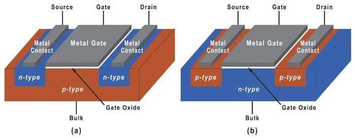
Overview of a PMOS (a) and NMOS (b). Image used courtesy of MKS
Before diving into Intel's patent application, let's do a quick review of how we got here and what a forksheet transistor is as Intel aims to leverage it moving forward.
Farewell FinFET: Shifting to "RibbonFET" and "MBCFETs"
Engineers initially developed the FinFET (fin field-effect transistor) architecture to improve channel control over planar transistors. However, as complementary metal-oxide-semiconductor (CMOS) scaling continued to create ever-smaller transistors, even FinFET's channel control became inadequate.
To further improve control of the transistor channel, the gate-all-around field effet transistor (GAAFET) was developed.
The GAAFET gate fully encloses the channel to both reduce leakage when the transistor is off and increase drive current when the transistor is on, which allows a continued reduction in the operating voltage.

A graph of the voltage reduction as a function of FET process technology. Screenshot used courtesy of Samsung
The nanosheet transistor is a type of GAAFET in which the channel is a planar sheet. Often, multiple nanosheet channels are stacked vertically to increase the effective width of the transistor and thereby provide additional drive current.
Last year, Intel has branded its nanosheet transistor technology RibbonFET and will be bringing it to market in its 20A process node using a 4-ribbon stack.
On the other hand, Samsung refers to its version as Multi-Bridge Channel FETs (MBCFETs) and is expected to be in production in their 3 nm node.
With a bit of background on the progress FET technology has pushed forward, let's take a look at forksheet FETs.
Hello Forksheet FETs: imec Leads the Charge
In 2019 at the International Electronic Device Manufacturing Conference, imec introduced its forksheet transistor concept.
This new FET added a self-aligned gate end dielectric wall to a stack of nanosheet transistors. Overall, the dielectric wall provided isolation between NMOS and PMOS nanosheet transistors, allowing more aggressive packing of the transistors in the X-Y dimensions.
By moving the transistors closer together, designers can improve switching speeds and reduce power consumption.
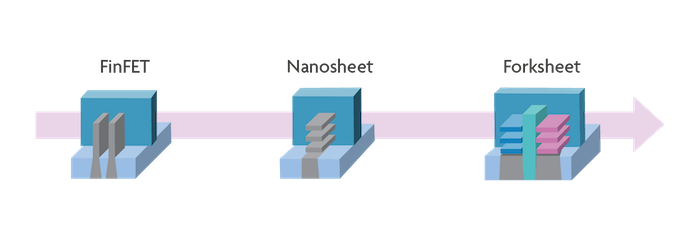
Semiconductor industry transistor evolution. Image used courtesy of imec
The forksheet design also claims to provide some manufacturing benefits when trying to stack more nanosheets vertically in a single nanosheet transistor. These process advantages were reported to include a simplified process for filling the work function gate metal.
Additionally, the imec analysis estimated that the forksheet FETs could provide a:
- 20% reduction in cell layout area
- 10% increase in speed (at constant power)
- 24% reduction in power reduction (at constant speed)
Something noteworthy to keep in mind is the naming conventions of these novel transistor designs, which continue to be an issue in the industry as these forksheet transistors are also referred to as "nanocombs" in the Intel patent.
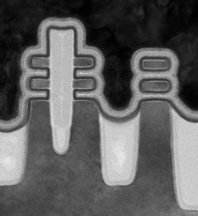
TEM image of forksheet FETs and a GAAFET. Image used courtesy of imec
In June of 2021, imec provided the first electrical demonstration of functional forksheet FETs at the Symposia on VLSI Technology and Circuits (VLSI 2021). The 22 nm NMOS and PMOS transistors were separated by only 17 nm, yet had different work function metal gates.
Stacked Forksheet Transistors
Even with the advantages of forksheet transistor manufacturing, the industry is yet again running up against the limits of 2D scaling.
Enter Intel's recent patent application for 3D stacked forksheet transistors. Intel proposes stacking NMOS on PMOS and PMOS on NMOS to reduce the cell size further.
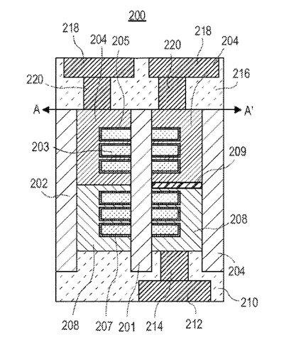
Intel’s stacked forksheet transistor concept. Image used courtesy USPTO and Intel
Fundamental CMOS logic like inverters and NAND and NOR gates regularly share the same electrical node for NMOS and PMOS gate pairs. Therefore, this type of stacking could improve packaging density which typically leads to increases in speed and reductions in power.
Within the patent application, Intel also describes an example process flow for manufacturing these stacked devices.
As with all modern CMOS processes, a simplified description includes numerous complex steps, including self-aligned double or quadruple patterning, dummy gate formation and removal, and selective epitaxial layer growth.
Though this article won't delve deep into the evaluation of this process, this new transistor technology claims to push forward a new range of applications.
Forksheet FETs: Opening a World of Applications
Intel's patent application for stacked forksheet FETs is a long way from a device demonstration, let alone high volume manufacturing. However, the potential benefits in speed, power, and density make it understandable that Intel may aggressively pursue this integration methodology.
Additionally, as the patent application notes, if they succeed, we may one day have stacked forksheet FETs in many areas such as:
- Processors (even crypto processors)
- Memory
- DSPs (digital signal processors)
- Touchscreen displays
- Wireless communication chips
- Global positioning system (GPS) devices
Those areas are but drops in the bucket that Intel points out in its list of uses. Intel will likely need future patent protection if its application is awarded.
Interested in other FET news? Read on in the articles down below.
