This article will discuss the basic concepts of clock gating and how it can be used to reduce the power consumption of synchronous digital systems.
Clock gating is a well-known technique for reducing the power consumption of a synchronous digital system. In this article, we’ll discuss the basic concepts of clock gating.
Register File: An Example Application for Clock Gating
In this section, we’ll examine the operation of a register file as an example application where clock gating can significantly reduce the power consumption. A processor utilizes a register file as a fast temporary storage device.
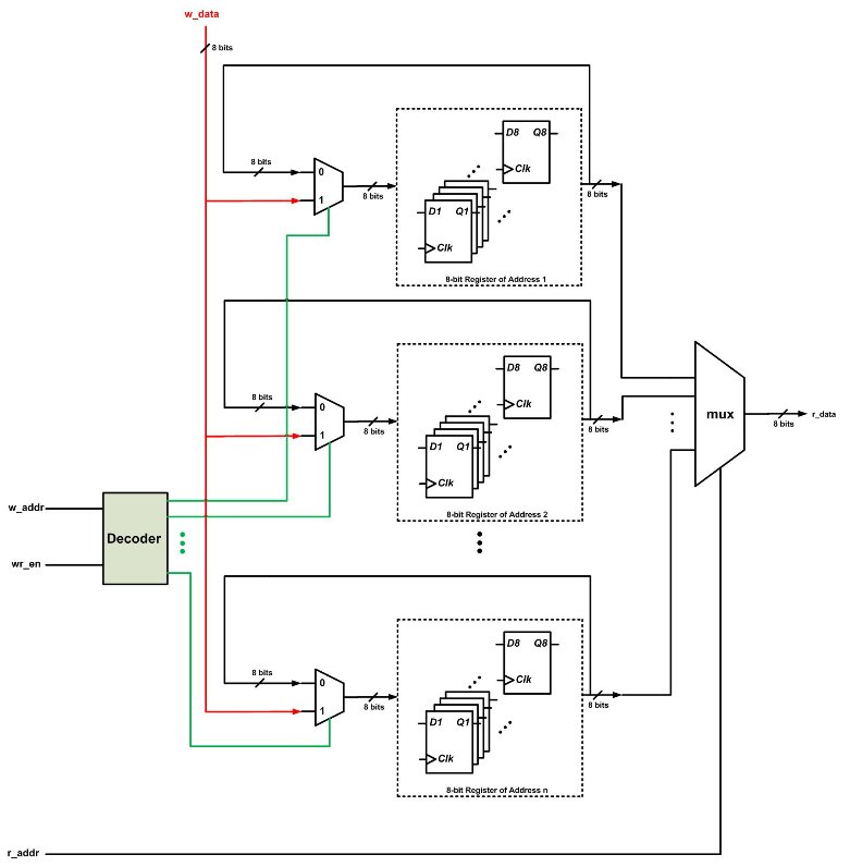
Figure 1. Block diagram of a register file. Click to enlarge.
As shown in Figure 1, the heart of a register file is an array of D-type flip-flops (DFFs). We can envision these DFFs as a two-dimensional array. In Figure 1, there are n rows where each row consists of eight DFFs. The FFs in each row are placed inside a dashed box. We can write an eight-bit data word to, or read an eight-bit data word from, any of these n rows.
To perform the write/read operation, we need to specify the target row. This is achieved by specifying an address for each row of the register file. Moreover, since only one operation, either write or read, is allowed at a time, we need another input to specify whether we are writing to or reading from the file. In Figure 1, the one-bit input wr_en, which stands for write enable, determines the operation type. When wr_en is high, we are writing; otherwise, the register file is in read mode.
In write mode (wr_en=1), the “decoder” block will choose one of the rows based on the value of the write address w_addr. This will set the select input of the target row multiplexer to one and w_data, which is the write data, will be passed to the row input. At the upcoming rising edge of the clock, w_data will be stored in the DFFs of the selected row.
To perform the read operation, we again need to select the target row. This is achieved using a multiplexer at the output of the register file. The select input of this multiplexer is connected to r_addr which specifies the read address. Moreover, during the read operation, we have to return the data stored in each row back to its input so that the content of the registers doesn’t change unintentionally at the clock edge. In other words, when in read mode, we are specifying the current value of a register as its next value. To this end, a two-input multiplexer is placed at the input of each row. During the read operation, the select input of all these multiplexers is logic low and, hence, the content of each DFF is returned to its input.
Read Mode Wastes Power
Read mode is not efficient from power consumption point of view. In this mode, the content of the register file doesn’t need to be updated; however, with each clock tick, we are updating the registers with their current value. This requires applying the clock signal to a large number of DFFs. Remember that the clock input of each FF introduces some parasitic capacitance (let’s call this capacitance ). Hence, for an n-by-8 array of DFFs, the clock input will see a parasitic capacitance of
Here, we have ignored the parasitic capacitance of the clock distribution network itself, though this capacitance can be significant.
Each time the clock signal switches from zero to one, the clock distribution circuitry charges to logic high. This requires drawing current from the power supply; the higher becomes, the more current we will need. How can we avoid charging this capacitance? During the read operation, the content of the register file must not change. The approach shown above ensures that the register values will not change, but we can achieve the same thing by simply switching off the clock signal. This technique, called clock gating, can significantly reduce power consumption. However, it can lead to serious problems too. Let’s take a closer look at this technique.
Clock Gating
Assume that we have decided to use a gated clock for the DFF shown in Figure 2. The main clock is ck and we have an enable signal, en, which determines when the DFF should operate (in the register file example, the write enable signal, wr_en, can be used for clock gating purposes). When en is logic high, the gated clock, gck, will be equal to ck. This is the basic concept of clock gating. But, what if en is logic low? Should gck be high or low in this case? What circuit should we use instead of the box labeled with the question mark in Figure 2?
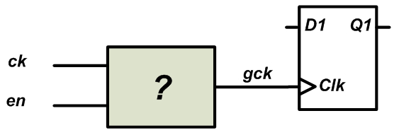
Figure 2
Since the DFF shown in Figure 2 is sensitive to the positive edge of the clock, we assume that the en signal too comes from devices that change state at the rising edge of the clock. For example, in Figure 3, the clock signal, ck, goes from low to high at t=t1; some time later, the en signal transitions to high at t=t2. The time difference t2-t1 corresponds to the delay of the circuitry that produces the en signal. As an example, we can assume that a particular output of a finite state machine (FSM) generates the en signal. In this case, t2-t1 will correspond to the delay of the FFs that store this particular state of the FSM plus the delay of the combinational circuit that generates the en signal from the FSM state (we are assuming that the system is synchronous and the FSM changes state with ck). Hence, the transitions of en will occur some time after the rising edge of ck.

Figure 3
Let’s use the above example waveforms to find a circuit that can generate an appropriate gated clock, gck, for Figure 2. From t2 to t4, the en signal is high and gck must be equal to ck. What if en is logic low? Should gck be high or low in this case? First, we assume that, for en=0, gck is set to low. Then, we’ll get the red waveform shown in Figure 4. To generate this waveform, we replace the unknown circuit of Figure 2 with an AND gate as shown in Figure 5.
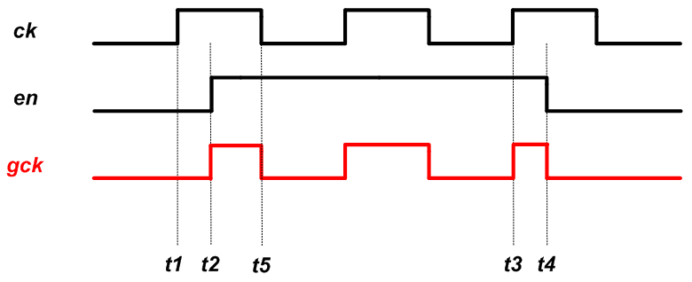
Figure 4

Figure 5
There are a few problems with this clock gating. First, do we really need a rising edge for gck at t=t2? One may think that the rising edge of gck at t=t2 is the delayed version of the rising edge of ck at t=t1; however, note that, at t=t1, we have en=0 and, hence, the clock edge of ck must not reach the FF. Thus, this gating arrangement produces an undesired rising-edge transition.
Another issue is that the pulse width from t2 to t5 is shorter than that of ck. A very short pulse can cause the DFF to malfunction. There is a third problem with this technique that we’ll discuss soon.
Let’s examine the next possibility: when en is logic high, the gated clock, gck, will be equal to ck but, for en=0, gck will be set to high. Then, we’ll get the green waveform shown in Figure 6. To generate this waveform, we can use the circuit shown in Figure 7.
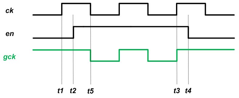
Figure 6

Figure 7
As you can see, unlike the gck of Figure 4, the gck generated in Figure 6 doesn’t have the rising edge at t=t2. With the circuit of Figure 7, a rising edge is presented to the DFF only when en is high and a rising edge occurs on ck. Moreover, the generated pulse width cannot be shorter than that of the original clock.
The clock gating of Figure 7 has another important advantage over that of Figure 5, namely, it is more resilient to glitches on the en signal. As discussed above, we assume that our synchronous system triggers changes at the rising edge of the clock. Also, we assume that the logic that generates the en signal has a delay that is less than half the period of ck. This means that en will start changing state right after the rising edge of ck (at t=t1) and will reach its final value before the next falling edge of ck, i.e., before t=t5. However, before reaching its final value, the en signal can have glitches. Let’s see what happens if we use clock gating with an enable signal that experiences undesired transitions. Figure 8 shows the example waveforms for the circuit of 5.
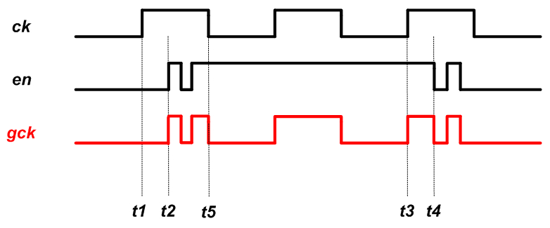
Figure 8
As you can see, the glitches on en are directly passed to the gated clock. These glitches can cause gck to have multiple rising edges for a single positive edge of ck, in some cases this can be disastrous, for example, assume that this gated clock is applied to a counter. The output of the counter will depend on the number of the rising edges of gck which, in turn, depends on the en glitches. Moreover, the main goal of using clock gating was to reduce the power consumption by eliminating unnecessary transitions of ck but, now, we are making the situation even worse because the en glitches are also introducing additional undesired transitions in the clock path. Examining the circuit of Figure 7, we observe that this circuit is resilient to glitches that happen during the high state of ck:
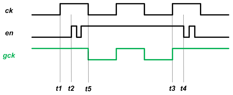
Figure 9
The above discussion shows that for a synchronous system in which the logic is driven by the rising edge of the clock, we should use the OR-based circuit of Figure 7. However, for a synchronous system in which the logic is driven by the falling edge of the clock, we should use an AND gate to generate the gated clock (see Section 1.10.5 of this book for details).
Clock Gating in FPGAs
Clock gating is a common technique used to reduce power consumption in the context of application-specific integrated circuit (ASIC) design. However, in FPGAs, we normally avoid gating the clock. This is mainly due to the fact that, in an FPGA, dedicated nets and buffers are utilized to appropriately route the clock signal to different parts of the chip. Clock gating can interfere with the clock distribution network, for example, by forcing the clock signal to go through a general-purpose lookup table. If clock gating is utilized in FPGAs, it’s up to the designer to check that the synthesized circuits are safe.
However, power optimization software packages can be used to apply the concepts of clock gating in order to reduce the power consumption of the circuit. For example, Xilinx has an option called “Intelligent Clock Gating” which uses the clock enable pin in a slice to neutralize superfluous switching activity. The technique is different from the classic clock gating discussed in this article because Intelligent Clock Gating doesn’t actually create new clocks. Instead, Xilinx’s technique uses clock enable pins of slices to disable registers that don’t contribute to the circuit’s operation for a given clock cycle. You can find details about this technique in this application note.
Summary
- Classic clock gating can significantly reduce power consumption. This can be done, for example, by switching off the clock signal for DFFs that don’t change state.
- For a synchronous system in which the logic is driven by the rising edge of the clock, we should use an OR gate to generate the gated clock. In this case, we’ll have correct timing along with resilience to glitches.
- For a synchronous system in which the logic is driven by the falling edge of the clock, we should use an AND gate to generate the gated clock.
- In FPGAs, classic clock gating is discouraged because it can lead to unexpected or undesired functionality.
To see a complete list of my articles, please visit this page.

