The design of a modern IC is a truly monumental undertaking, and IC design tools make the job possible.
EDA (electronic design automation)—also referred to as ECAD (electronic computer-aided design)—has become a standard in industry. Various software EDA tools are used to design systems, circuits, PCBs, and components. Perhaps nowhere are EDA programs more important, however, than in IC design.
In this article, we'll briefly introduce some EDA software tools from Cadence, Synopsys, and Mentor Graphics.
What Are EDA Programs Meant to Accomplish in IC Design?
A common focal point of EDA programs, as they exist today, is to link the various steps involved in smoothly getting from RTL to GDS.
RTL (register transfer level) is a model of a digital circuit defined in terms of the flow of digital signals and the logical operations down to the level of individual flip-flops.
GDS stands for graphic database system, and GDSII is the paramount database standard describing IC layout artwork. It is used to contain all the information describing the IC’s layout artwork and can be used for sharing between different tools and for building photomasks.
There are multiple steps along this road, and the key to producing great designs quickly is to integrate the individual steps for flawless hand-off. It is important to note that the various manufacturers handle this critical function in different manners. And, if an issue later in the design cycle calls for a change in an earlier phase, that, too, must be easily applied.
Of vital importance is the two-part Place and Route phase. Placing involves the optimal placement of the sub-blocks of the nascent IC, and routing is design of an optimal scheme of electrical interconnects between the sub-blocks.
The Synopsis Digital Toolset
Synopsys’ Digital Toolset is used for silicon chip design, verification, IP integration, and application security testing. Unlike previous generations of EDA, its Fusion Technology eliminates the former hard boundaries between synthesis, place-and-route and signoff, sharing integrated engines across the platform.
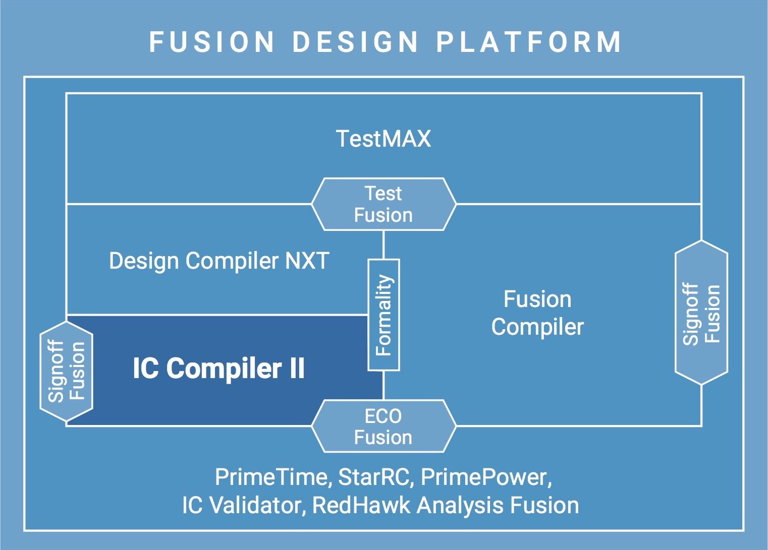
The Fusion design platform. Image from Synopsys
The Fusion design platform employs machine learning to enable better and faster results by speeding up computation-intensive analyses, predicting outcomes to improve decision-making, and leveraging past learning.
The cloud-based solution is available on Microsoft Azure, Amazon Web Services, and the Synopsys Cloud Solution.
The key to the fusion design platform is the solid back-and-forth coordination between:
- RTL Synthesis
- Physical Implementation (RTL-to-GDSII)
- Signoff (design verification)
- Physical Verification (design rules and manufacturability)
- Test Automation
IC Compiler II is Synopsys’ RTL-to-GDSII tool for place and route, across all types of ICs and process technologies. It spans 16/14nm, 12/10nm, 7/5nm, and sub-5nm geometries.
IC Compiler II enables designers to perform fast exploration and floorplanning with complex layout requirements. IC Compiler II can create bus structures, handle designs with n-levels of physical hierarchy, and can support multiply instantiated blocks (MIBs).
A design data mismatch inferencing engine analyzes the quality of inputs to deliver design insights even with “incomplete” data early in the design cycle.
Of great importance to designers, Synopsys collaborates closely with all the leading foundries to ensure that IC Compiler II can deliver support for both early prototype design rules and for the final production design rules.
Cadence: Virtuoso and Spectre
Cadence’s IC design tools include Virtuoso and Spectre. Like most of Cadence’s software tools, they are Linux-based and are run on servers. The tightly integrated tools are targeted largely, but not exclusively, at RFICs and RF modules.
Virtuoso
- Schematic editing of circuit
- Layout of circuit
- Design rule check
- Layout vs. schematic
Spectre
- DC, AC, and transient analysis
- S-parameter analysis for linear circuits
- RF analysis for non-linear circuits, including PSS (periodic steady state) and QPSS (quasi-PSS)
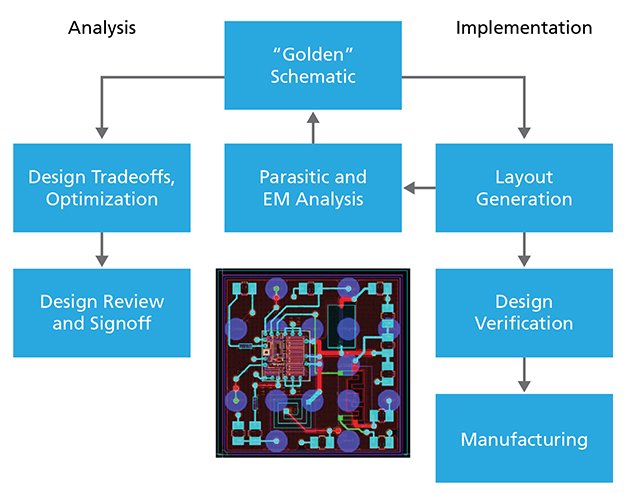
Virtuoso design flow. Image from Cadence
The Virtuoso Layout Suite GXL
The Virtuoso Layout Suite GXL consists of automatic layout engines for routing, layout optimization, module generation, and analog/mixed-signal floorplanning. This tool allows an engineer to create various designs (digital, analog, or mixed-signal) and implement them from chip level to device level.
Virtuoso ADE Product Suite
The Virtuoso ADE Product Suite is tightly linked to the Spectre Circuit Simulator as well as to the Virtuoso Suite. This tool is designed for the early stages of the circuit design cycle. Once a circuit block is up and running, it is tested, including its interactions with other blocks in the design.
The suite includes the Virtuoso ADE Verifier for design verification. The purpose here is to ensure that all the blocks from all the project’s designers coalesce to meet all the design specifications. Old manual methods for this vital step were and are a significant source of late-stage problems that negatively affect time to market.
Spectre Circuit Simulator
The Cadence Spectre Circuit Simulator provides SPICE-level simulation for analog, RF, and mixed-signal circuits. Tightly integrated with the Virtuoso custom design platform, it provides detailed analysis down to the transistor level.
The package provides statistical analysis to improve the manufacturability and yield of ICs without sacrificing time to market. Most importantly, Cadence employs foundry-certified device models so that manufacturability is considered early on in the design process.
SiP Layout
The SiP (system-in-package) Layout tool provides a constraint-driven and rules-driven substrate layout environment. This includes full 3D design visualization, verification, and editing capabilities.
Mentor Graphics – Tanner EDA
The Tanner EDA program automates the design, layout, and verification of analog/mixed-signal ICs, as well as MEMS. Note that digital IC design is covered by other Mentor tools, such as Tanner Digital Implementer for the physical design process.
Most Tanner modules are both Linux and Windows compatible.
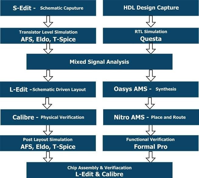
Mentor’s Analog Mixed Signal design flow. Image from Mentor.
The phases of this product’s operations include:
- Schematic capture
- Analog simulation
- Layout
- Physical verification
Tanner S-Edit Schematic Capture
Tanner S-Edit Schematic Capture is tightly integrated with simulation. This makes it easy to see results directly on the schematic. Designers can observe the small signal parameter of devices and view model parameters. Waveform cross-probing can be performed to view node voltages and device terminal currents or charges.
Extensive library support serves to maximize the reuse of IP developed in previous projects, or imported from third-party vendors.
Tanner T-Spice Simulation
For analog simulation, Tanner T-Spice Simulation presents circuit behavior characterized via DC/AC analysis, transient analysis, parameter sweeping, etc.
Tanner Waveform Viewer
Also for analog simulation, the Tanner Waveform Viewer is dynamically linked to Tanner T-Spice simulation and Tanner S-Edit schematic capture. Mentor notes that the tool can handle larger files ("10GB+"). It automatically calculates and displays FFT results.
Tanner L-Edit IC Layout
The Tanner L-Edit IC Layout is schematic-driven, imports netlists and automatically generates parameterized cells. DRC (design rule check) displays violations immediately, saving time.
Tanner Calibre One
Tanner Calibre One is used for physical verification and ensures that the layout is in actuality equivalent to the schematic. Layout-dependent effects are examined to be sure that they don’t impair the performance of the design. The tool serves to ensure ultimate manufacturability.
There are many companies offering EDA tools. We can’t cover them all in this small report, but here is just one more:
Analog Integrated Circuit Design Automation (AIDA) automates the design of analog and mixed-signal ICs. It focuses on efficiently automating repetitive design tasks. It does so partially by facilitating design reuse and by fast response to specification changes of analog cells.
The process of designing an IC is a vast undertaking. The design teams simultaneously working on the project can be located all over the world. The design can incorporate company IP and foundry IP as well as newly developed designs.
Problems can pop up late in the design phase, and for that reason, the most common factor in all IC design software is the tight linking together of all the components. That way, if a problem shows itself in the last stages of verification, it will be easy to change a schematic and to follow all the changes that then occur, and if necessary, compensate for them