Learn how to use the gridded ground technique to reduce noise in a double-sided PCB.
The ground planes of a multi-layer board can significantly improve the noise performance of a circuit. With a double-sided board, we usually cannot have a ground plane and we expect to have more noise and emissions. Due to this limitation, we prefer a multi-layer board unless the cost objectives force us to use a two-layer board.
Even though we don't have a ground plane with a two-layer board, there are still techniques that can be used to improve circuit performance. This article takes a look at the ground grid technique that allows us to implement an efficient ground circuit for a double-sided board.
How can a ground plane reduce board noise? In order to develop a better understanding of the operation of the “ground grid” technique, it will help you to first understand the function of a ground plane in a PCB. Please review my article on how a ground plane reduces board noise if need be before moving on.
What Is a Gridded Ground Plane?
A ground grid is created by a network of connections to ground across the PCB. For example, as shown in Figure 1, we can have some horizontal ground traces on the bottom layer of the board along with some vertical ground traces on the top layer. Moreover, there are vias at the intersections of the vertical and horizontal ground traces.
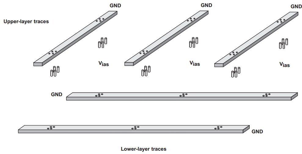
Figure 1. Image courtesy of TI.
How can the above technique create a low-inductance ground system? The grid in Figure 1 is a rather coarse one. A finer ground grid is shown in Figure 2 (the bottom and top ground traces are not distinguished). The signal trace connects the output of the gate in the top left corner to the input of the gate in the bottom right corner.
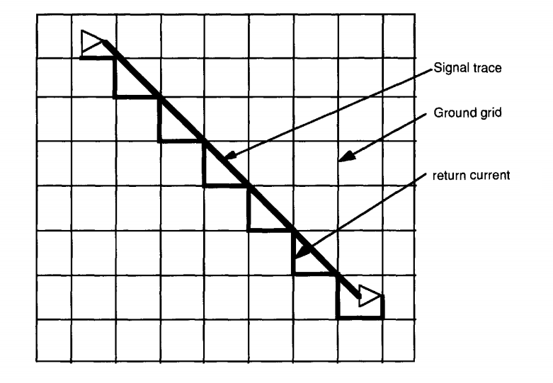
Figure 2. Image courtesy of EMC and the Printed Circuit Board.
As you can see, the current loop can be closed through the many alternative return paths that the ground grid provides. Although there are many return paths in parallel, most of the current will flow through the path closest to the signal trace to minimize the path inductance. A possible return path that can exhibit a relatively small inductance is shown in the figure.
Note that, with a ground grid, you may have to use several vias to route a signal trace across the PCB. This is shown in Figure 3 (it was not shown in the conceptual diagram of Figure 2).

Figure 3. Image courtesy of Introduction to Electromagnetic Compatibility.
Therefore, it’s better to have most of the top layer traces running vertically and most of the bottom layer traces running horizontally so that fewer vias are required.
How Effective Can It Be?
One way to examine the effectiveness of a ground system is measuring the ground noise voltage between the various ICs on a board. A study compared the voltage difference between the ground pins of the ICs of a two-layer board that uses a ground grid to that of a similar design with a single-point ground. The study shows that the ground grid can reduce the voltage difference between the ground pins of the ICs from 1000 mV to 100 mV (this was the best improvement between the various combinations of the ICs). According to this study, the board radiation was reduced by about 7 dB when the ground grid technique was applied. For more details about this research, please refer to Section 10.5.3 of Electromagnetic Compatibility Engineering by Henry W. Ott.
To achieve a significant reduction in the ground circuit inductance, a ground grid spacing of 0.5 in. or less should be used. In general, as the frequency of operation increases, we may need to use a finer grid to provide more parallel paths and reduce the ground system inductance. The ground grid technique is compatible with circuits operating up to 10 MHz; above this frequency a ground plane should be used.
Other Versions of the Ground Grid Technique
Different books and application notes have suggested slightly different versions of the ground grid technique. While the ground grid of Figure 1 relies only on the ground traces, the book High Speed Digital Design: A Handbook of Black Magic by Howard Johnson and Martin Graham suggests the grid shown in Figure 4.
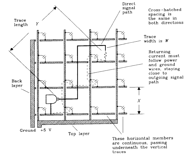
Figure 4. Image courtesy of Howard Johnson and Martin Graham from High Speed Digital Design: A Handbook of Black Magic.
In this case, the vertical ground traces on the top layer are replaced with power traces. The horizontal members are connected to ground. Note that these ground traces are on the bottom of the board and are continuous; they are not interrupted by the power traces on the top layer. The ground grid of Figure 4 will work because the AC return current can flow back to its source equally well along either the ground traces or the power traces. Since vias cannot be used in this scheme, we have to use bypass capacitors at the intersections of the vertical and horizontal traces. These capacitors should be of a high quality to let the current easily flow back to its driving gate.
We can also have ground and power traces on both the top and bottom layers. This is shown in Figure 5 below.
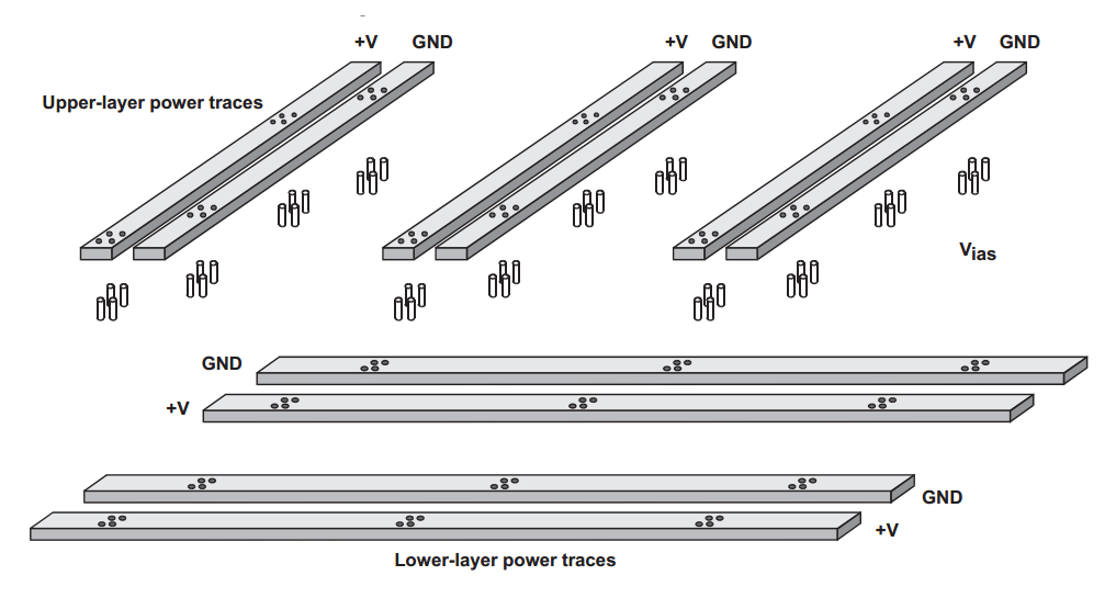
Figure 5. Image courtesy of TI.
This will take up more board space, but we expect it to exhibit a lower inductance because now the return current can flow through both the ground traces and the power traces. The part of the return current that flows through a power trace will use a bypass capacitor to reach a nearby ground trace through which it can flow back to a driving gate.
If board space limitations do not allow you to use wide traces, you can implement the grid using narrow traces. This is shown in Figure 6.
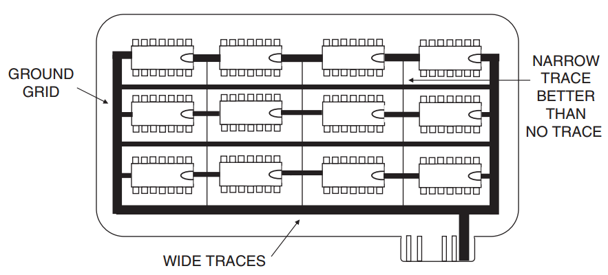
Figure 6. Image courtesy of Electromagnetic Compatibility Engineering.
A wide trace can provide lower resistance, which is important for low-frequency considerations; however, even a narrow trace can add many parallel paths to the grid system and decrease the ground inductance (a high-frequency consideration).
Conclusion
Ground path inductance can increase board noise through several different mechanisms. A multi-layer board allows us to have solid ground planes that can significantly reduce ground inductance. However, with a double-sided board, we have to resort to other techniques, such as a ground grid, to implement a low-inductance ground system. A study has shown that a ground grid can reduce emissions by about 7 dB and ground-voltage disparities by an order of magnitude.
To see a complete list of my articles, please visit this page.
