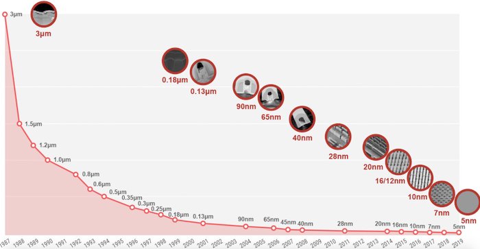
The semiconductor industry's history is largely the history of scaling down node sizes defined by Moore's Law. This trend, beginning roughly in the 1960s, has continued with seeming ease over the decades that followed, until recent years when the industry has hit a wall.
Around the 7 nm node, scaling became extremely difficult, as new considerations like quantum effects and fabrication challenges have limited our ability to scale as easily as we once did.

An example of TSMC's node scale. Image used courtesy of TSMC
Taking on this challenge, Samsung has made major news in the industry as it announced it had become the first to start production of a 3 nm process.
In this article, we'll look at some of the challenges in scaling, Samsung's new multi-bridge-channel FET (MBCFET) technology, and the news of its newest process node.
History of Scaling Down
As scaling of transistor node sizes started reaching extremes around the early 2010s, the industry began facing significant challenges in terms of MOSFET performance, control, and fabrication.
Specifically, as the transistor scaled down, concerns such as short channel effects and subthreshold leakages became greater as channel lengths decreased.
To address this, engineers had to replace conventional planar MOSFETs, and Intel introduced the solution in 2011 as the FinFET. The FinFET allowed for the effective channel width of the MOSFET to increase significantly, which ultimately helped control the short-channel behavior and the device's subthreshold leakages.

A planar (left) vs FinFET (right) architectures. Image used courtesy of Lam Research
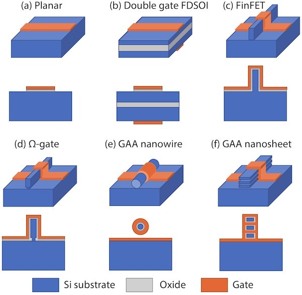
However, as scaling continued, FinFETs also needed to evolve. To continue using FinFET technology to realize performance gains while shrinking size, major factors have included fin width scaling for better gate controllability, fin pitch scaling for capacitance reduction, and fin height increases for DC increases.

The evolution of MOSFET architectures. Image used courtesy of Sun et al
Today, the industry has evolved to using gate-all-around (GAA) MOSFETs, which provide greater capacitive coupling between the gate and the channel. GAA FETs, today, are often based on nanowires, where a number of wire layers are piled up to increase the total channel width.
Despite this solution, most of the industry is struggling with a lack of process margin in areas such as fin etching, cutting, and leaning. This problem has been one of the largest challenges for the industry to reach beyond the 5 nm node.
Samsung Reaches 3 nm with MBCFET
Now, Samsung has broken through the barriers to continual scaling, as it has recently announced that it has begun production of its 3 nm process. According to Samsung, the key technology that has allowed it to reach this point is its newest MOSFET architecture, the MBCFET.
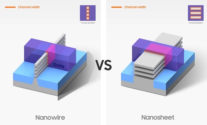
An MBCFET can be classified as a GAA technology; however, it deviates from the industry standard of using nanowires and instead uses a sheet-type structure with a greater width than a wire. By utilizing a nanosheet instead of a nanowire, MBCFETs can offer several key advantages, such as continuous channel width adjustment by controlling sheet width.
Along with this, the MBCFET could offer a structural change enabling all four sides of the device to act as a channel.

MBCFETs utilize nanosheets as opposed to nanowires. Image used courtesy of Samsung
Through these innovations, Samsung claims its MBCFET could offer lower operating voltages, higher current efficiencies (i.e., drive current capability), and high design flexibility. These advancements culminated in a new technology that allowed Samsung to begin successfully manufacturing on the 3 nm node.
According to Samsung, compared to the 5 nm process, its first-generation 3 nm process can reduce power consumption by up to 45%, improve performance by 23% and reduce the area by 16%. Goals for the future include a second-generation 3 nm node that will further reduce power consumption by up to 50%, improve performance by 30% and reduce the area by 35%.
Pushing Process Nodes Further
The industry has been fiercely competitive and struggling to reach the 3 nm node for years. With Samsung reaching 3nm in production, the company is marking a huge milestone for the semiconductor industry and creating hope for continual improvements moving forward.
