PCB stack-up refers to the arrangement of copper layers and insulating layers that make up a circuit board. The stack-up we choose can play a major role in board performance in several different ways. For example, a good stack-up can reduce the impedance of the board ground structure and limit the radiation and crosstalk.
This article looks at the common stackups for a four-layer board.
Stack-ups with Both Power and Ground Planes
Two common stack-ups for four-layer boards are shown in Figures 1 and 2. For these two boards, the order of the layers are exactly the same but their thickness is different. This might seem like a minor modification but we’ll see that an appropriate spacing between the different layers can improve board performance.

Figure 1. Image courtesy of Electromagnetic Compatibility Engineering.

Figure 2. Image courtesy of Electromagnetic Compatibility Engineering.
As you can see, both signal layers are next to plane layers (either a ground plane or a power plane). Therefore, the return current of a given signal can flow on an adjacent plane. This minimizes the current return path inductance by minimizing the loop area that is created by the current flow. A low-inductance return path improves noise performance and reduces board radiation (both differential and common-mode emissions).
Generally, a four-layer board can have about 20 dB less radiation compared to the same circuit implemented on a two-layer board. Keeping the signals close to solid planes is the key factor at play here. Hence, to further improve the noise and EMI performance, we can make the insulator between a signal layer and its adjacent plane even thinner. This simple trick gives us the improved stack-up shown in Figure 2, where coupling between the signal layers and the planes is increased at the cost of reducing the coupling between the ground and power planes. This may not be a serious disadvantage because actually neither of these two stack-ups provide sufficient plane-to-plane coupling. We’ll discuss this in greater detail in a minute. Note that the two stack-ups have the same overall board thickness.
The stack-ups of Figures 1 and 2 are commonly used, but they have two shortcomings, both of which arise from the fact that the ground and power planes are not close enough to each other and, consequently, there exists only a small interplane capacitance between them.
Drawbacks to the Conventional Four-Layer Stack-ups
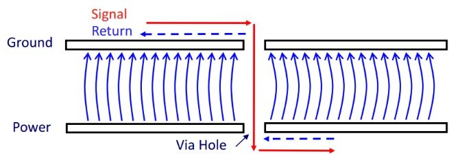
The first problem with the stack-ups in Figures 1 and 2 arises when a trace changes layer from layer 1 to 4 or vice versa. This is shown in Figure 3.

Figure 3. Image courtesy of Altium.
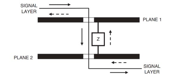
The figure shows that when a signal trace goes from layer 1 to layer 4 (the red line), the return current must change planes too (the blue line). If the frequency of the signal is high enough and the planes are close together, the return current can flow through the interplane capacitance that exists between the ground and power planes. However, the absence of a direct conductive connection for the return current creates an interruption in the return path, and we can envision this interruption as an impedance between the planes (see Figure 4).

Figure 4. Image courtesy of Electromagnetic Compatibility Engineering.
If the interplane capacitance is not large enough, the electric fields will spread over a relatively large area of the board so that the impedance between the planes reduces and the return current can flow back to the top plane. In this case, the fields created by this signal may interfere with the fields of nearby signals that change layers. This is not at all desired. Unfortunately, on a 0.062-in 4-layer board, the planes are placed far from each other (at least 0.020 in., as shown in Figures 1 and 2) and the interplane capacitance is small. Therefore, we’ll have the mentioned electric-field interference. This may not lead to a signal integrity problem, but we’ll certainly generate more EMI. That’s why when working with the stack-ups shown in Figures 1 and 2, we’d better avoid changing layers, especially for high-frequency signals such as clocks.
It is often good practice to add a decoupling capacitor close to a transition via to decrease the impedance that the return current experiences (see Figure 5). However, such decoupling capacitors are not effective with very-high-frequency signals because of their low self-resonant frequency. For an AC signal with frequency above about 200-300 MHz, we cannot rely on a decoupling capacitor to create a low-impedance return path. Therefore, we need both a decoupling capacitor (for below 200-300 MHz) and a relatively large interplane capacitance for higher frequencies.

Figure 5 Image courtesy of Altium.
The problem discussed above can be avoided by not changing the layer of a critical signal. However, the small interplane capacitance of a four-layer board leads to another serious problem: power delivery. A clocked digital IC usually needs large transient power supply currents. As the rise/fall time of the IC outputs decreases, we need to provide the energy at a higher rate. To provide a source of charge, we usually place decoupling capacitors very close to each logic IC. However, there is one problem: as we go beyond the self-resonant frequency, a decoupling capacitor cannot efficiently store and deliver energy because at these frequencies, a capacitor will act like an inductor.
Since most of today’s ICs have fast rise/fall times (about 500 ps), we need an additional decoupling structure that exhibits a self-resonant frequency higher than that of a decoupling capacitor. The interplane capacitance of a board can be an efficient decoupling structure provided that the planes are close enough to each other to provide sufficient capacitance. Hence, in addition to employing the commonly used decoupling capacitors, we prefer to have closely spaced power and ground planes to provide transient power for digital ICs.
Note that we normally don’t have a thin insulator between the second and third layers of a four-layer board because of the common board fabrication process. A four-layer board with a thin insulator between layers 2 and 3 will probably cost much more than a conventional four-layer board.
Two Improved Stack-ups
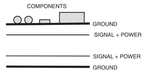
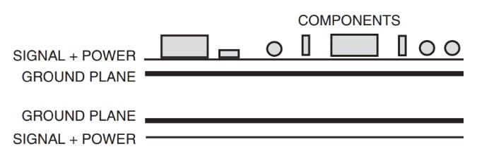
Figures 6 and 7 below show two improved stack-ups for four-layer boards.

Figure 6. Image courtesy of Electromagnetic Compatibility Engineering.

Figure 7. Image courtesy of Electromagnetic Compatibility Engineering.
As with the stack-ups of Figures 1 and 2, signal traces should be adjacent to a plane and the current return path inductance should be minimized. In this regard, the stack-up in Figure 6 may not be ideal because the mounted components will prevent us from having a solid ground plane on layer 1. Assuming that we can route most of the signal traces over solid parts of the ground planes, we observe that the insulator between signal layers and planes is thin, which is highly desirable.
The stack-ups in Figures 6 and 7 have two ground planes. This allows us to have a low-impedance ground structure and reduce common-mode radiation. Moreover, in Figure 6, the ground planes enclose the signal layers. Acting as a shield, the planes can contain the radiation from high-speed signal traces. We can even place stitching vias at the periphery of the board to connect the two ground planes together. This will create a Faraday cage and further contain the radiation. The planes of the stack-up in Figure 7 cannot act as shields.
With these two stack-ups, we don’t have a power plane. We can either use power pours or a gridded power structure. If we can route the signal and power traces and mount the components on one layer (layer 1), then the stack-up in Figure 7 can be employed (this stack-up has solid ground planes). However, if we do not have enough space for all of these, we can use the stack-up in Figure 6.
Although these two stack-ups don’t have solid power planes, the power pours are in close proximity to the ground planes. As a result, the power pours and the ground planes will create a relatively large capacitance that can act as a decoupling structure at high frequencies. Rick Hartley, a well-respected PCB designer, presents measured data confirming that the decoupling between the power pours and planes of Figures 6 and 7 outperforms the decoupling provided by the ground and power planes of a conventional four-layer board (Figures 1 and 2). Using the decoupling structure of the improved stack-ups along with the usual decoupling capacitors, we can more easily provide transient power for high-speed digital ICs.
Finally, with the improved stack-ups of Figures 6 and 7, high-speed signals can change layers because all the signals are referenced to ground planes (in the conventional stack-ups, the signals were referenced to either a ground plane or a power plane). As a result, we can place a plane-to-plane via close to a transition via to provide a low-impedance path for the return current. For more information, please refer to Section 16.3.3 of the book Electromagnetic Compatibility Engineering.
Conclusion
In this article, we examined several different stack-ups for four-layer boards. We saw that stack-up choice can play a major role in board performance in several different ways. A good stack-up can reduce the impedance of the board ground structure and limit radiation and crosstalk. Additionally, the board stack-up can affect transient power delivery and our signal routing strategy when changing layers.
To see a complete list of my articles, please visit this page.
