In today’s designs, complex circuit issues such as latch-up, noise immunity, floating pins, cross-power-domain verification, and leakage current require verification techniques that can combine physical and electrical information to understand more complex connectivity and greater design context. Without such checks, designers cannot adequately verify the robustness of a schematic or layout design to ensure that circuits will operate as designed and intended, and that the circuitry is well-protected against potential electrical failures.
Traditional ERC vs. Advanced ERC
Traditional electrical rule checking (ERC) typically verifies elemental electrical design rules, using basic connectivity and device information to find issues such as floating wells and bad device construction. Such ERC execution has usually been enabled with design rule checking (DRC) and layout versus schematic (LVS) verification tools. However, more complex circuit issues are now being checked, including latch-up, noise immunity, floating pins, cross-power-domain verification, and leakage current, among others.
Given the combination of advanced semiconductor process technology, the introduction of the system-on-chip (SoC), the existence of multiple power domains in today’s designs, and the need for in-context data during checking, ERC has become more and more challenging, to the point where traditional verification tools are no longer sufficient. Advanced ERC has become an important part of design verification for any integrated circuit (IC) chip design.
How is advanced ERC different? These checks typically require in-context information to verify the robustness of a schematic or layout design from the perspective of electrical engineering, ensuring that circuits will operate as designed and intended, and that the circuitry is well-protected against potential electrical failures. Advanced ERC violations can result in reduced yield, or worse, potential circuit malfunction or electrical failure after product delivery. Finding and correcting these errors is critical to product reliability and market success [1-5].
Why not just use a simulation tool? Unfortunately, simulation tools such as SPICE are only helpful to a limited extent, because they require precise set-up to expose subtle design issues. They also lack the scalability needed for today’s large SoC designs, which often contain billions of transistors.
Verification of these advanced electrical design rules requires electronic design automation (EDA) tools that understand more complex connectivity and greater design context. For example, some rule checks may involve one or more of the following situations:
- Conditional device on and off scenarios
- Propagation of varying voltage levels through MOS devices
- Vectored inputs at voltage supply pins
- Identification of un-driven gates
- Circuit recognition (e.g., level-shifters and current mirrors)
Advanced ERC
Let's look at the some of the rule checks advanced ERC helps with in more detail.
Conditional Voltage Propogation
Electrical overstress (EOS) occurs when the electrical power or signals applied to a circuit or a device exceed normal operating conditions. An EOS check flow traces voltage propagation from the input pins of a circuit design, and flags any devices that are connected to higher-than normal voltages. However, an EOS flow based on traditional DRC and LVS tools usually only comprehends simple voltage propagation scenarios, in which a MOS device is always either on or off. Such a simplistic approach often results in the EOS check flow becoming too pessimistic, flagging false violations that result in wasted time during debugging.
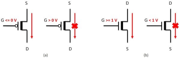
To obtain accurate voltage propagation information across a circuit design, the voltage propagation algorithm must be able to control the “ON” and “OFF” status of MOS devices based on the voltages at their gate pins, instead of simply assigning an “ON” or “OFF” status to MOS devices regardless of their input voltages. Implementing a conditional voltage propagation control allows engineers to specify the conditions under which a MOS device will be turned on or off, as shown in Figure 1. During conditional voltage propagation, each individual MOS device can be turned on or off, based on the voltage at its gate pin.

Figure 1. Conditional voltage propagation: (a) The PMOS is “ON” when the voltage at gate pin is <= 0 V, and “OFF” when the voltage at gate pin is > 0 V. (b) The NMOS is “ON” when the voltage at gate pin is >= 1 V, and “OFF” when the voltage at gate pin is < 1 V.
Some advanced ERC tools also support the definition of an attenuated voltage propagation from the source pin to the drain pin of a PMOS, based on the voltage at the gate pin, to mimic the voltage drop across a PMOS device.
Pin-to-Pin Resistance
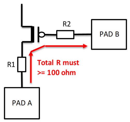
During circuit design, designers must frequently check for and avoid unexpected low-resistance paths between input pins. For example, sneak paths are one of the major challenges in memory resistor (memristor) design at both circuit and architecture levels [6]. A sneak path is an unplanned low-resistance path for electrical current that is in parallel to an intended path. Designers must ensure the resistance value between two input pins, or between an input pin and a device terminal, is within design specification, as shown in Figure 2.

Figure 2. Pin-to-pin resistance: The resistance along the path from PAD A to PAD B, which includes R1 and R2, must be equal to or greater than 100 ohms.
Advanced ERC enables designers to easily evaluate the resistance value between two input pins, or between an input pin and a device terminal, and flag any potential low-resistance sneak paths. The paths being evaluated for resistance value can include resistors, as well as other devices such as diodes.
Finding Undriven Gates
During the initialization or power-down of power domains, some gate pins of MOS devices have no definitive voltage values, and become un-driven. While some un-driven gates can be intentional, unintentional un-driven gates can result in erroneous behavior in a chip.
A typical example involves gates connected to the output pin of a tristate buffer. When a tristate buffer is used to drive output load in a circuit, its output pin can be “electronically” disconnected from its output circuitry through an enable pin (EN) when required. When this disconnect occurs, the output pin of the tristate buffer is neither at a logic HIGH or LOW, but instead has an output state of very high impedance, which is often referred to as High-Z or floating. Figure 3 shows a tristate buffer and its truth table, which describes the relationship between its input and output voltages. If the EN pin of the tristate buffer is at zero volts, the output pin Y of the tristate buffer has no definitive voltage value and becomes floating. Subsequent gates connected to pin Y then become un-driven.

Figure 3. When the EN pin of a tristate buffer with the given truth table is at 0 volts, its output pin Y becomes floating, and subsequent gates connected to pin Y become un-driven.
Advanced ERC can check and flag these un-driven gates, helping designers ensure there are no unintentional floating gates in the circuits. To implement these checks, the ERC tool must support vectored input voltages at input pins of a circuit design, as well as the Unified Power Format (UPF) standard for specifying power intent in power optimization for EDA tools [7]. Designers can evaluate voltage propagation across the entire circuit design based on different scenarios of input voltages, and flag the gate pins that are un-driven.
High-Voltage Level-Shifter
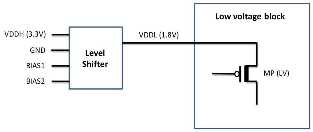
Some circuits contain core logic transistors operating at a low voltage, while also having an interface to high-voltage I/O transistors. In such cases, level-shifter circuits are used to scale down the voltage from the high I/O voltage, as shown in Figure 4. Designers must verify the existence of a level shifter between two different voltage levels, and ensure that low-voltage MOS devices are not accidentally connected to a high voltage, which can cause an EOS condition.

Figure 4. Level shifters moderate voltage changes to prevent device damage or circuit failure. This level shifter converts VDDH (3.3V) into VDDL (1.8V).
Some ERC tools can use pattern matching functionality to search for custom pre-defined level shifter configurations in the design, as well as provide fast verifications of the existence of level shifters and their connectivity. This capability can also flag MOS devices with potential EOS risks.
Hot Carrier Injection
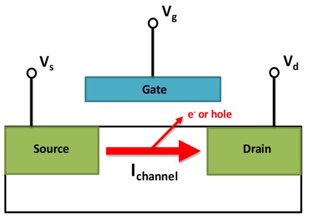
When transistors switch, some high-energy (“hot”) electrons or holes may gain sufficient kinetic energy to overcome potential barriers and get injected into the gate oxide region, where they become trapped, as shown in Figure 5. These accumulation of electrons or holes can cause gradual damage to the gate oxide, leading to a threshold voltage shift, and eventually circuit failure.

Figure 5. In HCI, channel current gets injected into gate oxide.
The traditional aging simulation used to identify potential hot carrier injection (HCI) risk does not work for SoC designs, due to runtime and capacity limitations. However, designers can use some simple voltage conditions to flag PMOS devices that are susceptible to HCI, as shown in equation (1):
Vsg,max ≥ Vsd,min
where Vsg,max = Vs,max - Vg,min is the maximum voltage between source and gate of the PMOS, and Vsd,min = Vs,min - Vd,max is the minimum voltage between source and drain of the PMOS [8].
Based on input voltages, advanced ERC tools understand the voltage scenarios at terminals of PMOS devices, and can calculate the maximum and minimum voltages between source and gate (or source and drain) of PMOS devices. They can then flag PMOS devices that are susceptible to HCI.
The above conditions are just some of the challenging electrical design rules that can be checked using advanced ERC tools like the Calibre™ PERC™ reliability platform from Mentor, a Siemens business. Compared to traditional ERC flows, context-aware checking enables designers to perform more sophisticated checks on their circuit designs that require complex device and connectivity information.
Advanced ERC Flow Implementation
To be truly useful, automated circuit verification must not only be able to understand and apply the design context information required by advanced ERC, but also deliver the scalability needed to run efficiently on large SoC designs.
Some advanced ERC tools can run ERC checks on either a schematic netlist (SPICE) or a layout design database (GDSII or OASIS). When taking a schematic netlist as input, the tool must traverse the netlist hierarchy to flag ERC violations on nets or devices. For ERC checks that involve voltage propagation, it must read voltage information on input pins of a circuit design, and propagate voltages throughout the design based on voltage propagation rules defined by users.
When using layout design data as input, the tool must first run an LVS layout extraction to obtain the device and connectivity information from the layout design. Depending on the ERC tool used, designers may or may not have to write their own decks to extract the device and connectivity information from a layout design. In addition, if the ERC tool is integrated into the company’s sign-off LVS flow, many ERC checks can be seamlessly integrated and run in parallel with the LVS compare process to provide faster turnaround times (TAT).
ERC is a Critical Step in Design Verification
At advanced semiconductor process nodes, ERC is becoming a critical component of design verification. Without a full set of advanced ERC checks, companies risk releasing products that do not perform as designed, or experience premature failure in the field.
At the same time, the verification of many of these advanced electrical design rules requires EDA tools like the Calibre PERC reliability platform that understand complex connectivity and device information, including circuit recognition, a capability that traditional physical verification tools lack.
With advanced ERC tools that can provide automated sign-off quality circuit verification for ESD, EOS, multiple power domains, advanced ERC, and other complex reliability concerns, design companies can deliver reliable, robust products on schedule and on budget, while providing the performance and product life the market demands.
References
[1] M. Hogan, “Improve Reliability with Accurate Voltage-Aware DRC,” Mentor, a Siemens Business. Sept., 2013.
[2] M. Hogan, “Improving Design Reliability by Avoiding Electrical Overstress,” Mentor, a Siemens Business. Sept., 2013.
[3] D. Medhat, “Protecting Against IC Reliability Failures With Automated Voltage Propagation,” Mentor, a Siemens Business. July, 2017.
[4] M. Hogan, “Automated and Context-Aware Latch-Up Checking With the Calibre PERC Reliability Platform,” Mentor, a Siemens Business. June, 2017.
[5] F. Yoder, “Automated Body Bias Validation for High Performance, Low Power Electronics,” Mentor, a Siemens Business. Oct., 2017.
[6] M.A. Zidan, H.A.H. Fahmy, M.M. Hussain, K.N. Salama, “Memristor-based memory: The sneak paths problem and solutions,” Microelectronics Journal, vol. 44, issue 2, pp. 176-183. February 2013.
[8] S.H. Renn, J.L. Pelloie, and F. Balestra, “Hot-Carrier Effects in Deep Submicron SOI MOSFETs,” 1996 IEEE International SOI Conference Proceedings, Sanibel Island, FL, USA, 1996, pp. 60-61.
doi: 10.1109/SOI.1996.552493
Industry Articles are a form of content that allows industry partners to share useful news, messages, and technology with All About Circuits readers in a way editorial content is not well suited to. All Industry Articles are subject to strict editorial guidelines with the intention of offering readers useful news, technical expertise, or stories. The viewpoints and opinions expressed in Industry Articles are those of the partner and not necessarily those of All About Circuits or its writers.
