Demands for high-performance compute (HPC) capability have been steadily on the rise for the past several years, especially with the commercial adoption of 5G edge services for AI/ML applications. Over the last couple of years, 2.5D and 3D die-stacking is slowly replacing single IC package designs in some applications like 3D NAND memory.
Samsung Electronics' foundry division recently announced a generational improvement of their advanced package technology I-Cube, called 'I-Cube4', a 2.5D interposer package containing four high-bandwidth memory (HBM) modules tied directly to a logic die.
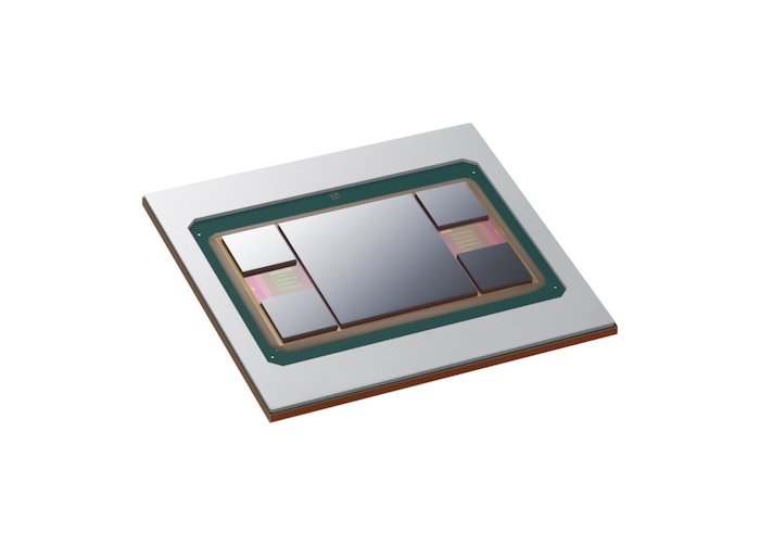
Samsung's new four HBM + Logic I-Cube4 technology. Image used courtesy of Samsung Electronics
With this new announcement, a few questions come to mind: what is 2.5D technology, how does it enable HPC, and does it have any drawbacks compared to traditionally packaged integrated circuits?
HPC Counts Improvements Through Gflops/Watt Metrics
Excluding Cray's in-development Frontier Supercomputer, power efficiency is nearly linear in supercomputing applications. In 2016, Nvidia's DGX SaturnV was the most energy-efficient at just under 10 Gflops/watt.
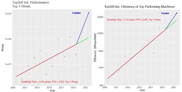
A graph of performance (left) and efficiency (right) curves for the top 500 supercomputers currently. Image [modified] used courtesy of Koomey et all and AMD
Projections from a 2019 AMD report show that Gflops/watt should nearly triple by 2022 with the Frontier (compared to the DGX SaturnV).
Intel and AMD are also producing data center processors outside of supercomputing with 40 and 64 cores, respectively. With higher core density processors, comes significant thermal management challenges, which are the reality of today.
Further commercialization of 2.5D interposer technology could ease some of these performance constraints by improving the speed of access and reducing power consumption. To do that, it is necessary to understand the general basics of 2.3D technology.
The Basics of 2.5D Interposer Technology
High-compute designs require high-bandwidth memory as close to the logic die as possible. However, parasitic electrical parameters reduce performance regardless of how densely a traditional PCB is packed.
What's worse, these parasitics plague designers at all levels of design, from board level right down to silicon fabrication. Based on a solid physics background and empirical simulation and testing, good design practice is critical to design 2.5D interposer technology.
Interposer technology is similar to how traditional integrated circuits are connected on copper layers laminated to a PCB substrate but are significantly smaller inside a single package.
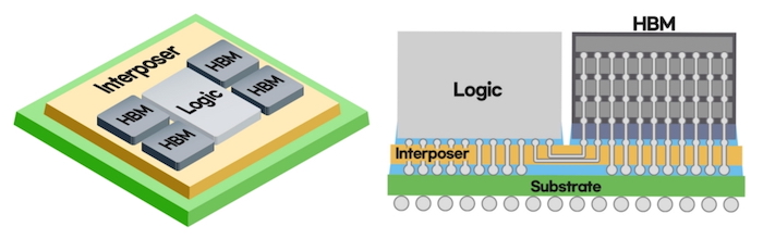
A render of the I-Cube4's 2.5D advanced packaging structure. Image used courtesy of Samsung Electronics
In the case of the I-Cube4, the four HBM and logic die are set on top of the interposer. The interposer then provides the connectivity between the HBM and logic. With this design, the designer must weigh out the benefits with the disadvantages.
2.5D Benefits and Challenges
2.5D technology offers a host of benefits. Three key benefits could be fundamental to selecting this particular technology for your designs: footprint efficiency (space savings), speed, and power reduction.
The first benefit, the advanced integration in a single footprint, enables the second two benefits. The interconnections are tiny, thus reducing propagation times between the dies and eliminating some of the power consumed in the traces. Though this can be an important benefit to a designer, one issue is parasitics.
There is no surprise to engineers or physicists, but the parasitics that plague PCB designers are also present at the wafer level. As mentioned, interposer technology is modeled after printed circuit boards.
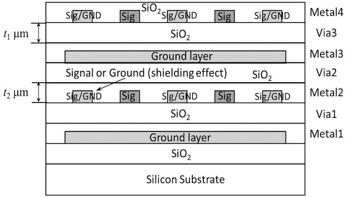
Interposer stack up for high-bandwidth memory interfacing. Screenshot [PDF] used courtesy of Bo Pu
Beyond the electrical issues, thermal management is another critical issue to address. Interposer layers are less than 100 µm thick and are prone to warpage. According to Samsung Electronics, their experience in this domain has allowed them to overcome this limitation through changes to their fabrication materials.
2.5D Interposer Signal Integrity & PCB Relationships
Signal integrity in HBM channels is one critical parameter [pdf] being evaluated by researchers at Samsung. Eye diagrams, through masks, are one of the best methods for assessing the jitter performance of high-speed interfaces.
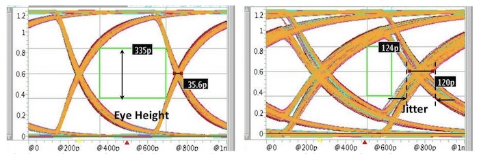
Eye masks for a 6mm trace (left) and 9 mm trace (right). Image courtesy of Bo Pu
In both stripline and microstrip, the researchers compared two different layer topologies to evaluate the best performance. Nominally, S-G-S-G and S-S-S-S structures were compared with various trace widths and distances between traces.
The research team found that both structures performed similarly at 3 µm, which was 3x over their minimum distance between traces. This result follows a "rule-of-thumb" called the 3W rule, which aims to reduce the inductive and capacitive coupling between traces by separating signal traces by three times their width; however, simulation and modeling should be used for high-speed designs.
Samsung Electronics’ Focuses on HPC
Moonsoo Kang, senior VP of Foundry Market Strategy, sees the I-Cube4 development as essential to support their customers.
He says, "with the explosion of high-performance applications, it is essential to provide a total foundry solution with heterogeneous integration technology to improve the overall performance and power efficiency of chips."
Samsung Electronics' Foundry division has additional advanced package technologies for applications in mobile and other leading-edge technologies. The new I-Cube4 brings additional high-bandwidth memory capability, allowing for enhanced AI workloads, networking, graphics, and HPC.
Interested in other advancements in the world of high-performance computing? Read more down below.
ARMv9: the Long-awaited High-Performance Computing Architecture
Data Buffers to the Rescue for Bandwidth-Burdened Server and Cloud Applications
IEEE Awards TSMC for 7nm Leadership. Where Is TSMC Going Next?