Recent developments in software are significantly outpacing those in hardware, at least at the industry level. This outpacing results from the slower design lifecycle of ICs, which generally takes years from academia to industry, and then years from industry to market. On the other hand, software can have the luxury of rapid iteration, where changes can happen overnight.

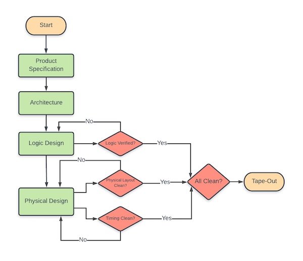
An example of an ASIC design flow. Image from AnySilicon
Many of the world’s largest tech companies have been interested in how IA could play into the IC design process. For example, some companies are NVIDIA looking into using machine learning (ML) for IC design, and Cadence focusing on using AI in simulation tools to improve verification and power analysis.
Another company that has been showing interest in this concept since last year is Google. With this AI trend for IC design in mind, this article will discuss how Google is looking to use AI to expedite the IC design process and its implications on everyday EEs.
Google’s AI for IC Floorplanning
One of the most time-intensive aspects of any IC design is the chip floorplanning, which is the layout of individual circuit blocks to optimize power, area, performance, and signal integrity while meeting design constraints.
Recently, Google's paper discussing the use of "deep reinforcement learning" in chip placement, a proposed solution to speeding up IC design, was published in Nature.

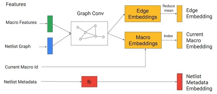
Process flow of Google’s IC AI. Image used courtesy of Google
Google's solution works using a specially developed edge-based graph neural network, taking the chip's netlist as an input and generating edge and macro embeddings as output. This output is then is passed to a feedforward neural network which outputs a learned representation of useful chip features. This process is repeated continually, optimizing for average wire length, congestion, area, power, and performance.
As stated in a previous article, Google found that this process can potentially perform chip floorplanning in a fraction of the time required by humans. In addition, this technique could also analyze much more design possibilities than humans, enabling it to spit out chip designs that are cheaper and smaller in less time.
Though this possible solution sounds like a way to help speed along the IC design process and, in general, help EEs in their workflows, it does raise some questions. One question is, how could this affect electrical engineers?
Implications for Engineers
In many fields, people are afraid of AI taking away jobs, and electrical engineering is no exception; however, the question is: is this fear legitimate?
The first thing to consider is that often, as is the case with Google, these design AIs replace lower-level design concerns. Thus, a general rule of thumb may be that if something has the potential to be automated, it likely is not something that requires a depth of knowledge and may not be a good use of the engineer's time.
From this perspective, this increasing automation can be viewed as a good thing for EEs, freeing them up to focus on more crucial aspects of design. However, more involved stages in the IC design flow often require more profound expertise, application-specific knowledge, and years of training, making it unlikely to be automated by AI (at least as it stands today).

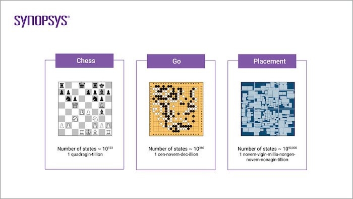
Chip placement is significantly more difficult than Go, which has only recently been solved by AI. Image from Synopsys
On the other hand, people who work in fields requiring less expertise may fear their work being replaced by automation, which is a legitimate concern. However, no matter how good AI gets, IC design is still too expensive and error intolerant to let a computer do without an eye test and sign off from a human engineer.
More likely than losing jobs, layout engineers will see their roles shift from performing much of the physical layout to analyzing, validating, and confirming the design completed by AI software.
What are your thoughts on AI streamlining the IC design process? Are there any processes or parts of your workflow that you would like to see become automated? Let us know in the comments down below.
