White Paper Overview
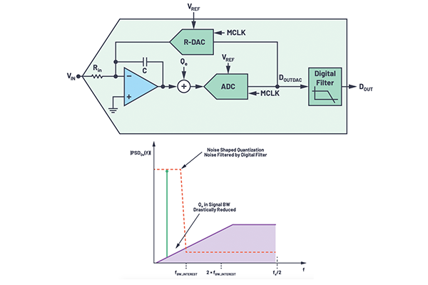
This article will explain continuous-time sigma-delta (CTSD) ADC technology in a less traditional approach, enabling signal chain designers to envision a new class of easy to use precision ADC technology as a simple system that interconnects a few well-known components. In Part 1, we highlighted the key challenges of incumbent signal chain designs that can be simplified significantly with a precision CTSD ADC, as it maintains continuous-time signal integrity while achieving the highest precision. Now, the question is what’s behind the CTSD architecture that enables it to achieve these advantages?
The traditional approach of explaining the concept of CTSD technology is by first understanding the basics of a discrete-time sigma-delta (DTSD) modulator loop and then substituting the discrete-time loop elements with equivalent continuoustime elements. While this method gives an in-depth understanding of sigma-delta functionality, we aim to provide a more intuitive understanding behind the inherent advantages of precision CTSD ADCs. To begin, we will outline a step-by-step approach to building a CTSD modulator loop starting with the widely known closed-loop inverting amplifier configuration and combining it with an ADC and a DAC. Finally, we will evaluate the basic sigma-delta functionality from the circuit we build.

